
Oct 12, 2019 (Nanowerk News) Scientists from Tokyo Metropolitan University have created a new layered superconducting material with a conducting layer made of bismuth, silver, tin, sulfur and selenium (Scientific Reports, "Bulk superconductivity in a four-layer-type Bi-based compound La2O2Bi3Ag0.6Sn0.4S5.7Se0.3"). The conducting layer features four distinct sublayers; by introducing more elements,...
Nanotechnology Now – Press Release: GLOBALFOUNDRIES Brings New Level of Security and Protection on 22FDX Platform for Connected Systems:22FDX security solution aims to protect against physical tampering and attacks for cellular Internet of Things (IoT) devices

Home > Press > GLOBALFOUNDRIES Brings New Level of Security and Protection on 22FDX Platform for Connected Systems:22FDX security solution aims to protect against physical tampering and attacks for cellular Internet of Things (IoT) devicesAbstract:GLOBALFOUNDRIES® (GF®), the worlds leading specialty foundry, announced today that it is working with Arm® to...
These new soft actuators could make soft robots less bulky
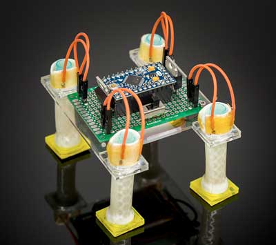
Oct 11, 2019 (Nanowerk News) Engineers at the University of California San Diego have developed a way to build soft robots that are compact, portable and multifunctional. The advance was made possible by creating soft, tubular actuators whose movements are electrically controlled, which makes them easy to integrate with small...
Nanotechnology Now – Press Release: GLOBALFOUNDRIES Acquires Smartcoms PDK Engineering Team to Expand Worldwide Design Enablement Capacity: Acquisition strengthens overall process design capabilities and expands the companys footprint in Europe

Home > Press > GLOBALFOUNDRIES Acquires Smartcoms PDK Engineering Team to Expand Worldwide Design Enablement Capacity: Acquisition strengthens overall process design capabilities and expands the companys footprint in EuropeAbstract:GLOBALFOUNDRIES® (GF®), the worlds leading specialty foundry, announced today that it has acquired the PDK (Process Design Kit) engineering team from Smartcom...