| Jul 17, 2023 |
|
(Nanowerk News) A new technology being pioneered at Caltech is allowing researchers to “evolve” optical devices and then print them out using a specialized type of 3D printer. These devices are made of so-called optical metamaterials that derive their properties from structures so small they are measured in nanometers, and they may allow cameras and sensors to detect and manipulate properties of light in ways not previously possible at small scales.
|
|
The work was conducted in the lab of Andrei Faraon, the William L. Valentine Professor of Applied Physics and Electrical Engineering and appears in the journal Nature Communications (“3D-patterned inverse-designed mid-infrared metaoptics”).
|
 |
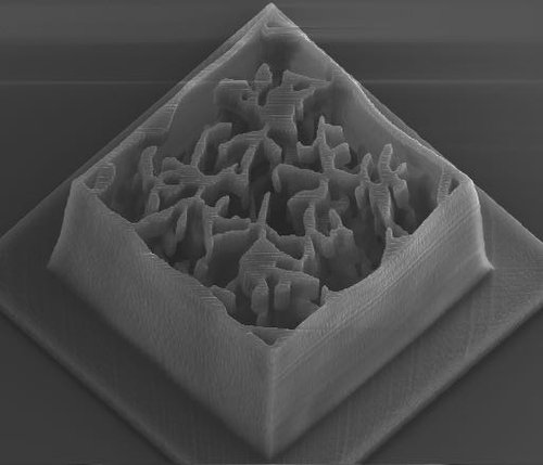
| SEM image of a fabricated device. It measures 5 µm from top to bottom. (Image: Caltech)
|
|
This isn’t the first time Faraon has developed optical metamaterials, but he says it is the first time these materials have been pushed into three dimensions.
|
|
“Generally, most of these things are done in a thin layer of material. You take a very thin piece of silicon or some other material and you process that to get your device,” he says. “However, [the field of] optics lives in a three-dimensional space. What we are trying to investigate here is what is possible if we make three-dimensional structures smaller than the wavelength of light that we are trying to control.”
|
|
As a demonstration of the new design technique, Faraon’s lab has created tiny devices that can sort incoming light, in this case infrared, by both wavelength and polarization, a property that describes the direction in which the light waves vibrate.
|
|
Though devices that can separate light in this way already exist, the devices made in Faraon’s lab could be made to work with visible light and small enough that they could be placed directly over the sensor of a camera and direct red light to one pixel, green light to another, and blue light to a third. The same could be done for polarized light, creating a camera that can detect the orientation of surfaces, a useful ability for the creation of augmented and virtual reality spaces.
|
|
A glance at these devices reveals something rather unexpected. Whereas most optical devices are smooth and highly polished like a lens or prism, the devices developed by Faraon’s lab look organic and chaotic, more like the inside of a termite mound than something you would see in an optics lab. This is because the devices are evolved by an algorithm that continually tweaks their design until they perform in the desired way, similar to how breeding might create a dog that is good at herding sheep, says Gregory Roberts, graduate student in applied physics and lead author of the paper.
|
|
“The design software at its core is an iterative process,” Roberts says. “It has a choice at every step in the optimization for how to modify the device. After it makes one small change, it figures out how to make another small change, and, by the end, we end up with this funky-looking structure that has a high performance in the target function that we set out in the beginning.”
|
|
Faraon adds: “We actually do not have a rational understanding of these designs, in the sense that these are designs that are produced via an optimization algorithm. So, you get these shapes that perform a certain function. For example, if you want to focus light to a point—so basically what a lens does—and you run our simulation for that function, you most likely will get something that looks very similar to a lens. However, the functions that we are targeting—splitting wavelengths in a certain pattern—are quite complicated. That’s why the shapes that come out are not quite intuitive.”
|
|
To turn these designs from a model on a computer into physical devices, the researchers made use of a type of 3D printing known as two-photon polymerization (TPP) lithography, which selectively hardens a liquid resin with a laser. It’s not unlike some of the 3D printers used by hobbyists, except it hardens resin with greater precision, allowing structures with features smaller than a micron to be built.
|
|
Faraon says that the work is a proof of concept but that with a bit more research, it could be made with a practical manufacturing technique.
|


