| Nov 15, 2019 |
|
(Nanowerk News) A newly discovered phenomenon in a flexible semiconductor could affect its promise for electronic devices.
|
|
Two-dimensional materials – those either only an atom or layer thick – display a number of interesting properties and could form the foundation for a range of new devices. One of these materials, molybdenum disulfide (MoS2), has shown an unusual flexibility that could make it attractive as a semiconducting component of bendable electronics.
|
|
In a new study (ACS Nano, “The Effects of Atomic-Scale Strain Relaxation on the Electronic Properties of Monolayer MoS2“) from the U.S. Department of Energys (DOE) Argonne National Laboratory and Temple University, scientists have discovered an intriguing new behavior in MoS2 at the atomic level as it is stretched and strained, like it would be in an actual flexible device.
|
|
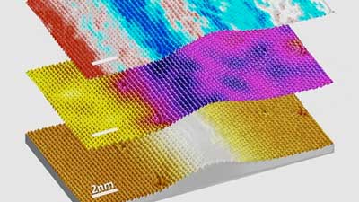
After straining a film of the material grown on graphite, the researchers noticed that the formerly two-dimensional sheet of MoS2 would slip, relaxing the strain. This, in turn, formed a rippled pattern at a larger scale that translated into an altered electronic structure within the individual atoms.
|
 |
| Scanning tunneling microscopy topography of a rippled MoS2 single layer as a result of strain relaxation (bottom). The corresponding dI/dV map at the valence band edge (middle), and the strain map (top) are overlaid. (Image: Argonne National Laboratory)
|
|
You can think of it like stretching a rubber band, said Argonne nanoscientist Saw-Wai Hla, an author of the study. “After you release the tension, the rubber band snaps back together even more tightly than its initial position.
|
|
The ripple pattern remains after the strain is removed, and leaves the material looking like a rug that has been bunched up as the material loses its total two-dimensionality. Introducing the ripple through strain could be either deleterious or helpful to the functioning of an actual flexible electronic device, according to Hla, who explained that while an unintentional strain relaxation would likely impair the material, a directed strain response could achieve precisely targeted electronic behavior in MoS2.
|
|
For an example of this behavior, since MoS2 is a semiconductor, the crystalline lattice exhibits what scientists call a band gap – a range of states that electrons cannot occupy. By straining the material, the researchers saw that they could shrink the band gap. Having different band gaps in a material is essential in case you want to do things like create a screen that can display different colors, Hla said.
|
|
Because the ripples can be introduced not just one at a time but in periodic succession, the potential has emerged for researchers to design certain regions of the material to have relatively lower band gaps and thus conduct electricity more easily.
|
|
“If you can artificially produce these ripples in these specific patterns, you can artificially produce a channel of conductance, said Argonne postdoctoral researcher Daniel Trainer, the first author of the study. “Being able to functionalize a material like this can have a lot of applications, like wearable electronics or foldable screens, especially on this very small scale.
|
|
These applications may include areas outside of flexible electronics as well. Two-dimensional materials are of interest to people working on things ranging from quantum computation to catalysts to sensors, Hla said. “Understanding this two-dimension materials could allow us to make a big impact as we work toward tailoring its electronic behavior.
|
|
The MoS2 straining experiment was performed at Argonnes Center for Nanoscale Materials, a DOE Office of Science User Facility. The researchers used scanning tunneling microscopy to look at the atomic positioning and behavior within the material.
|


