Reconfigurable superconducting nanobridges allow spatial control over quantum and classical states, enabling flexible layouts for nanoscale quantum circuit design.
(Nanowerk Spotlight) In superconducting research, geometry is not just a detail—it defines how the material behaves. Traditional approaches, constrained to flat films and planar devices, have enabled decades of progress in electronics and quantum technologies. Yet these systems are increasingly limited by their own geometry. Magnetic fields, supercurrents, and quantum vortices are all governed by how the material is shaped. When confined to two dimensions, the possibilities for manipulating these phenomena are inherently restricted.
This geometric constraint has prompted a growing effort to investigate superconductivity in three dimensions. Researchers have long studied the influence of curvature and topology on superconducting states in theory, but building suitable structures has been a challenge. Some early approaches relied on rolling thin films into coils or helices. These revealed some novel effects—such as geometry-induced phase transitions and enhanced detector sensitivity—but they were limited in design complexity. What was needed was a method to sculpt arbitrary 3D geometries with nanometer precision and electrical integration.
Recent advances in direct-write nanofabrication have made this possible. Focused electron beam induced deposition (FEBID), a technique originally developed for additive nanomanufacturing, allows researchers to construct free-standing nanoscale architectures in three dimensions. By scanning an electron beam over a surface in the presence of a gaseous precursor, FEBID enables the controlled deposition of metallic or semiconducting materials with high spatial resolution.
Published in Advanced Functional Materials (“Reconfigurable Three-Dimensional Superconducting Nanoarchitectures”), the work by a team at the Max Planck Institute for Chemical Physics of Solids and collaborating European institutions reports the creation and investigation of a fully three-dimensional superconducting nanostructure using focused electron beam induced deposition. The study demonstrates new methods of controlling superconducting states through geometric confinement, revealing effects that arise directly from the spatial architecture of the material.
These insights establish a foundation for more adaptable superconducting technologies, including applications in quantum circuits and magnetic sensing.
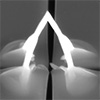
The team’s nanostructure is a bridge-like network made of tungsten-carbide (W-C), fabricated directly onto gold contacts using FEBID. As shown in Figure 1a, the device consists of four legs connected at the top by two converging nanowires, forming a sharp vertex with an internal angle of about 60 degrees. This setup enables electrical probing across the vertex while maintaining full three-dimensional connectivity. Each leg has a diameter of about 200 nanometers, situating the structure between the superconducting coherence length (approximately 5 nm) and the London penetration depth (around 850 nm). This size range puts the system in an intermediate regime, where superconducting behavior is shaped by both quantum and geometrical constraints.
Fabrication and characterization of 3D superconducting nanostructures. a) Schematic of the FEBID of 3D nanoarchitectures. b) SEM image of the W–C nanobridge deposited using FEBID. The diameter D of the nanobridge leg is ≈200 ± 15 nm. c) Temperature dependence of the resistance of the nanobridge under a magnetic field perpendicular to the substrate, from 0 T to 7 T, measured with I = 100 nA. The dashed line indicates the upper critical magnetic field. d) Upper critical magnetic field as a function of temperature. Data are fitted to a power-law equation μ0Hc2(T) ∼ (1 – T/Tc)n, identifying an intermediate regime of superconductivity. e) With the dimensions of the nanostructure lying between the coherence length and penetration depth, ξ << D << λ. (Image: Reprinted from DOI:10.1002/adfm.202506057, CC BY)
Measurements confirmed that the device enters a superconducting state below 5 K. When the team mapped its response to magnetic fields, they observed an upper critical field that did not follow the behavior typical of bulk or one-dimensional systems. Instead, the field-dependence of the superconducting transition fit a power law with an exponent characteristic of a geometry-influenced intermediate regime. This suggests that the physical dimensions of the nanowires, relative to the fundamental superconducting length scales, play a decisive role in determining the system’s behavior.
A key feature of superconductivity is the presence of quantized magnetic vortices when the material is exposed to a magnetic field. These vortices carry magnetic flux and interact with one another, with boundaries, and with imperfections in the material. In this study, the researchers confirmed that vortices could not only exist but also move within the 3D nanostructure. Using non-local voltage measurements, they demonstrated that vortices propagate through the conduit region of the structure, generating measurable voltage signals at remote contacts. This propagation confirms long-range interactions between vortices across the curved geometry, extending the concept of vortex dynamics from planar films into three-dimensional paths.
Further analysis using time-dependent Ginzburg–Landau simulations revealed that the vortices inside the nanobridge do not remain straight. Instead, they curve to accommodate the geometry of the structure and the applied magnetic field. The degree of curvature varies with field strength and orientation, illustrating a kind of “softness” in the vortex structure. At lower fields, the vortices are more flexible and curved; at higher fields, they become straighter and stiffer. This field-dependent curvature influences how easily the vortices can be pinned—a factor crucial for stability in superconducting circuits.
The geometry also introduces a distinct anisotropy in the superconducting state. When the magnetic field is rotated relative to the nanobridge, the critical field at which superconductivity disappears changes. The researchers found that this critical field could vary by nearly 30 percent depending on the field angle. This anisotropy is not due to material properties—microscopy showed the deposited W-C was isotropic—but to how the vortices align with the structure. Vortices prefer to align with the applied field in the bulk of the material, but at the surface, they are constrained to meet the boundary at right angles. This interplay creates a directional dependence in the system’s superconducting limits.
One of the most striking consequences of this anisotropy is the ability to create spatially distinct superconducting and non-superconducting regions within a single device. At certain field orientations, one leg of the nanobridge transitions to a resistive state while the other remains superconducting. This results in a controllable coexistence of quantum and classical behavior, effectively enabling localized switching within a continuous structure. This dynamic could be useful for designing multi-functional superconducting devices where different regions perform different tasks under the same external conditions.
The research also uncovered a reconfigurable weak link within the structure. Weak links are regions where superconductivity is suppressed, allowing a Josephson current—an essential ingredient in many quantum circuits. Normally, these links are built into the device during fabrication, using constrictions or material variations. In this 3D nanobridge, however, the weak link appears at the vertex only when the magnetic field is aligned to enhance the local perpendicular component. When the field is rotated, the weak link disappears, and the device behaves as a uniform superconductor. This makes the weak link tunable, not fixed, adding a degree of freedom for circuit design and reconfiguration.
The authors envision several applications for these findings. The FEBID technique allows for the rapid prototyping of complex 3D structures, including multi-terminal junctions and interconnected superconducting networks. These could serve as the building blocks for next-generation quantum processors, neuromorphic systems, or sensors with directional selectivity. The ability to define, modify, and remove superconducting regions through external control rather than physical alteration offers a versatile platform for adaptive electronics.
Perhaps most importantly, this study provides a direct method to explore how curvature, confinement, and connectivity influence superconducting behavior. The findings illustrate that three-dimensionality is not just a structural feature—it’s a tuning mechanism. As fabrication techniques continue to mature, it will become increasingly possible to design superconductors where the function is embedded not just in the material, but in the shape itself.
Get our Nanotechnology Spotlight updates to your inbox!
Thank you!
You have successfully joined our subscriber list.
Become a Spotlight guest author! Join our large and growing group of guest contributors. Have you just published a scientific paper or have other exciting developments to share with the nanotechnology community? Here is how to publish on nanowerk.com.