| Mar 16, 2022 |
|
(Nanowerk News) Photoresist-based patterning strategies have been standardized for decades since the invention of photolithography. However, there are still major challenges in the processing of certain functional structures.
|
|
For example, the standard resist-based high resolution patterning process usually requires point-by-point exposure of the target resist structures, leading to extremely low throughput and an unavoidable proximity effect when defining multiscale patterns, high-energy beam irradiation is easy to cause damage to the materials, and the negative-tone-resist-based lift-off process is challenging, stc.
|
|
Recently, the journal National Science Review (“Resist Nanokirigami for Multipurpose Patterning”) published the research results of Professor Duan Huigao’s research group from Hunan University.
|
|
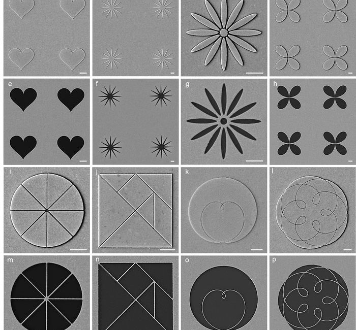
The team proposed and demonstrated a new resist patterning stratgy “resist nano-kirigami”. The outline of the target structure is exposed on the resist, and the excess resist film is selectively mechanically stripped.
|
 |
| (a-d) and (i-l) Multiscale metal micro-nano positive-type structures with sharp features or extremely small gaps; (e-f) and (m-p) the corresponding inverse metallic structures after lift-off. All scalebars: 1 µm. (Image: Science China Press)
|
|
Compared with traditional electron beam lithography, this scheme has the following core advantages:
|
|
It can effectively reduce the exposure area in the manufacturing process (for example, for a disc structure with a radius of 400 µm, the exposure area of this scheme can be reduced by 5 orders of magnitude compared to the traditional electron beam lithography strategy), which greatly improves the processing efficiency and achieves efficient fabrication of cross-scale “macro-micro-nano” complex functional structures that are difficult to achieve by traditional solutions.
Only the outlines of the target structure in the positive resist PMMA are exposed, both the positive- and negative-tone can be obtained by selective peeling of the PMMA.
|
|
The strategy provides a new patterning solution that expands the family of lithography techniques and will play a significant role in fabricating multiscale functional structures.
|


