| Jun 29, 2022 |
|
(Nanowerk News) Berkeley engineers have created a new type of semiconductor laser that accomplishes an elusive goal in the field of optics: the ability to maintain a single mode of emitted light while maintaining the ability to scale up in size and power. It is an achievement that means size does not have to come at the expense of coherence, enabling lasers to be more powerful and to cover longer distances for many applications.
|
|
A research team led by Boubacar Kanté, Chenming Hu Associate Professor in UC Berkeley’s Department of Electrical Engineering and Computer Sciences (EECS) and faculty scientist at the Materials Sciences Division of the Lawrence Berkeley National Laboratory (Berkeley Lab), showed that a semiconductor membrane perforated with evenly spaced and same-sized holes functioned as a perfect scalable laser cavity. They demonstrated that the laser emits a consistent, single wavelength, regardless of the size of the cavity.
|
|
The researchers described their invention, dubbed Berkeley Surface Emitting Lasers (BerkSELs), in a study published in the journal Nature (“Scalable single-mode surface emitting laser via open-Dirac singularities”).
|
 |
| Schematic of the Berkeley Surface Emitting Laser (BerkSEL) illustrating the pump beam (blue) and the lasing beam (red). The unconventional design of the semiconductor membrane synchronizes all unit-cells (or resonators) in phase so that they are all participating in the lasing mode. (Image: Boubacar Kanté group)
|
|
“Increasing both size and power of a single-mode laser has been a challenge in optics since the first laser was built in 1960,” said Kanté. “Six decades later, we show that it is possible to achieve both these qualities in a laser. I consider this the most important paper my group has published to date.”
|
|
Despite the vast array of applications ushered in by the invention of the laser — from surgical tools to barcode scanners to precision etching — there has been a persistent limit that researchers in optics have had to contend with. The coherent, single-wavelength directional light that is a defining characteristic of a laser starts to break down as the size of the laser cavity increases. The standard workaround is to use external mechanisms, such as a waveguide, to amplify the beam.
|
|
“Using another medium to amplify laser light takes up a lot of space,” said Kanté. “By eliminating the need for external amplification, we can shrink the size and increase the efficiency of computer chips and other components that rely upon lasers.”
|
|
The study’s results are particularly relevant to vertical-cavity surface-emitting lasers, or VCSELs, in which laser light is emitted vertically out of the chip. Such lasers are used in a wide range of applications, including fiber optic communications, computer mice, laser printers and biometric identification systems.
|
|
VCSELs are typically tiny, measuring a few microns wide. The current strategy used to boost their power is to cluster hundreds of individual VCSELs together. Because the lasers are independent, their phase and wavelength differ, so their power does not combine coherently.
|
|
“This can be tolerated for applications like facial recognition, but it’s not acceptable when precision is critical, like in communications or for surgery,” said study co-lead author Rushin Contractor, an EECS Ph.D. student.
|
 |
| Schematic showing the Dirac cones. Light is emitted synchronously from the entire semiconductor cavity as a result of the Dirac point singularity. (Image: Boubacar Kanté group)
|
|
Kanté compares the extra efficiency and power enabled by BerkSEL’s single-mode lasing to a crowd of people getting a stalled bus to move. Multi-mode lasing is akin to people pushing in different directions, he said. It would not only be less effective, but it could also be counterproductive if people are pushing in opposite directions. Single-mode lasing in BerkSELs is comparable to each person in the crowd pushing the bus in the same direction. This is far more efficient than what is done in existing lasers where only part of the crowd contributes to pushing the bus.
|
|
The study found that the BerkSEL design enabled the single-mode light emission because of the physics of the light passing through the holes in the membrane, a 200-nanometer-thick layer of indium gallium arsenide phosphide, a semiconductor commonly used in fiber optics and telecommunications technology. The holes, which were etched using lithography, had to be a fixed size, shape and distance apart.
|
|
The researchers explained that the periodic holes in the membrane became Dirac points, a topological feature of two-dimensional materials based on the linear dispersion of energy. They are named after English physicist and Nobel laureate Paul Dirac, known for his early contributions to quantum mechanics and quantum electrodynamics.
|
|
The researchers point out that the phase of light that propagates from one point to the other is equal to the refractive index multiplied by the distance traveled. Because the refractive index is zero at the Dirac point, light emitted from different parts of the semiconductor are exactly in phase and thus optically the same.
|
 |
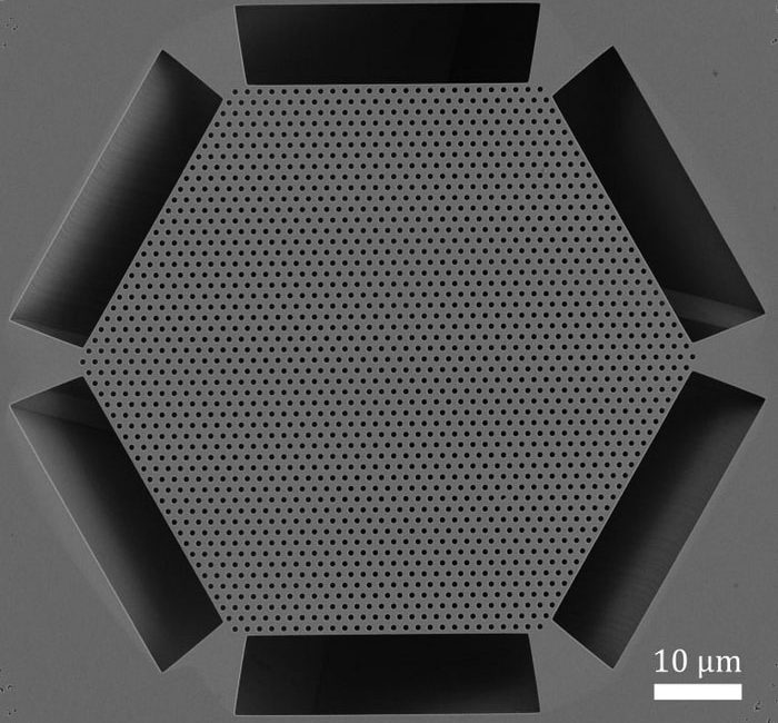
| Top view of a scanning electron micrograph of the Berkeley Surface Emitting Laser (BerkSEL). The hexagonal lattice photonic crystal (PhC) forms an electromagnetic cavity. (Image: Boubacar Kanté group)
|
|
“The membrane in our study had about 3000 holes, but theoretically, it could have been 1 million or 1 billon holes, and the result would have been the same,” said study co-lead author, Walid Redjem, an EECS postdoctoral researcher.
|
|
The researchers used a high-energy pulsed laser to optically pump and provide energy to the BerkSEL devices. They measured the emission from each aperture using a confocal microscope optimized for near-infrared spectroscopy.
|
|
The semiconductor material and the dimensions of the structure used in this study were selected to enable lasing at telecommunications wavelength. Authors noted that BerkSELs can emit different target wavelengths by adapting the design specifications, such as hole size and semiconductor material.
|


