| Mar 11, 2022 |
|
(Nanowerk News) Current computer and telecommunication technologies use electrical charges (electrons) and light (photons) to transport information. However, a breakthrough in this field could be brought about by the introduction of mechanical vibrations –phonons– as a means of transferring data, in combination with the other two.
|
|
In order to establish the basis for a new information technology, the researchers involved in the PHENOMEN project worked for almost four years on the development of a phonon-based signal processing system that could be incorporated in standard electronic chips.
|
|
The outcomes of this study have been recently published in a paper in ACS Photonics (“Room-Temperature Silicon Platform for GHz-Frequency Nanoelectro-Opto-Mechanical Systems”) introducing a proof-of-concept technology platform for the integration of phononic, photonic and radio-frequency (RF) electronic signals, which can be operated at ambient conditions and is fully compatible with CMOS technology. These remarkable results open new avenues for information processing and transport, not only in current IT applications, but also in future quantum networks.
|
|
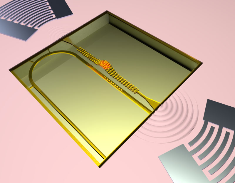
The researchers engineered a coherent phonon source using the opto-mechanical coupling mechanism, namely the interaction of radiation pressure forces with a resonator. The microscale resonator was designed to simultaneously sustain co-localised optical and mechanical modes.
|
|
The phonon source results from an opto-mechanical interaction involving competing mechanisms: one arising from the photo-generated carriers in the resonator and the other from the temperature variation of the resonator impacting its optical properties. This interaction leads to the generation of coherent vibrations, i.e., acoustic waves in-phase with each other.
|
 |
| Schematics of the silicon platform for GHz NEOMS. (Image: ICN2)
|
|
The core material used to maximize the opto-mechanical interaction is nanocrystalline silicon (nc-Si), a technology developed at VTT –instead of standard crystalline silicon (c-Si)–, which provides various advantages, such as: flexibility in tuning optical, mechanical and thermal property of the system; and increased affordability, since the components can be fabricated on standard silicon wafers.
|
|
The conversion of electrical signals into mechanical waves is achieved by combining silicon with aluminum nitride (AlN), which is a piezoelectric material –i.e. a material able to produce electricity upon application of mechanical stress. Both solutions represent a great innovation in the design and fabrication of NOEMS.
|
|
This novel silicon-compatible platform for nano-electro-opto-mechanical systems, which allows converting electric signals into optical ones via mechanical waves (and the other way around), was shown to operate at radio-frequencies (up to a few GHz) and at room temperature, thus it can be incorporated in CMOS fabrication processes. Therefore, it has the potential to become a ground-breaking solution for new, multifunctional and multi-signal technologies for information transmission and processing, both in the classic and the quantum domain.
|
|
The key components of this NEOMS platform were developed by a team of researchers from the Catalan Institute on Nanoscience and Nanotechnology (ICN2, Barcelona, Spain), CNR-Nano (Pisa, Italy), the Polytechnic University of Valencia (Spain) and the VTT Technical Research Centre (Espoo, Finland).
|
About the PHENOMEN project
|
|
PHENOMEN was a project funded by the European Union in the highly competitive H2020 FET-Open call 3 and coordinated by ICREA Prof. Dr Clivia Sotomayor Torres, head of the ICN2 Phononic and Photonic Nanostructures Group. Launched in 2016, it brought together three leading research institutes —the Catalan Institute of Nanoscience and Nanotechnology (ICN2), the Italian National Research Council (CNR-NANO Pisa, Italy), the VTT Technical Research Centre of Finland (VTT, Espoo, FInland)—, three internationally recognised universities –the Polytechnic University of Valencia (UPVLC, Spain), The Polytechnic University of Marche (UNIVPM, Italy), the Science and Technology University of Lille (USTL, France)– and an industrial partner –MENAPiC S.A.S (Lille, France). Together, they combined complementary expertise in photonics, phononics, optomechanics, electrical engineering, integration, nanofabrication, theory and modeling, instrumentation and application of detectors.
|
|
The goal of the PHENOMEN project was to harness the potential of combined phononics, photonics and radio-frequency (RF) electronic signals to lay the foundations of a new information technology. Specifically, it aimed to propose an implementation of in-chip phononic circuits based on opto-mechanical cavities working at ambient conditions. The platform developed will complement current state-of-the-art electronic and photonic circuitry by extending the frequency range of the signals and will rely on fully CMOS compatible materials.
|


