| Dec 13, 2022 |
|
(Nanowerk News) Superconducting nanotechnology is a rapidly developing field with a series of promising applications in the field of new quantum technologies such as advanced superconducting quantum processors based on qubits with Josephson tunnel junctions.
|
|
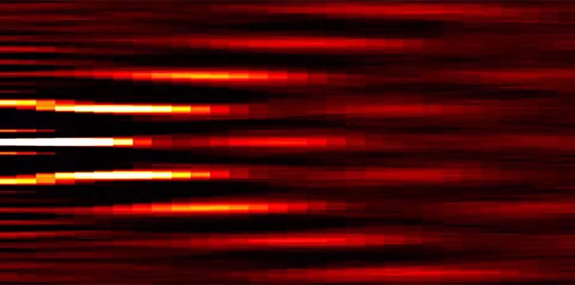
Recently, an international team of researchers – with participation of Leibniz Institute of Photonic Technology (Leibniz IPHT) – has demonstrated and published yet another quantum mechanical effect in superconductors – the photon assisted coherent quantum phase slip effect in a very thin superconducting nanowire. The effect is revealed as the formation of current steps on the current-voltage characteristic subject to microwave radiation (Nature, “Quantized current steps due to the a.c. coherent quantum phase-slip effect”).
|
|
This effect has been theoretically predicted more than thirty years ago and hints of the current steps of this type have been previously observed in small size Josephson junctions. Switching from a Josephson junction to a superconducting nanowire made of thin films of high-quality niobium nitride allowed the researchers to observe sharp and distinct steps on the current voltage characteristic located at current values In = 2efn, where 2e is the electric charge of a so-called Cooper pair of two electrons, f the frequency of microwave radiation, and n as an integer number, denoting the step order.
|
This fascinating effect can be potentially used for various applications like, for example, radiation detection or emission. However, the main potential application of it is the development of a metrological current standard. Indeed, at the first current step exactly one Cooper pair is transferred through the nanowire per one period of microwave radiation.
|
|
The current steps originate from the quantum coherent tunneling of a single vortex (a localized magnetic field corresponding to a single flux quantum) across the nanowire, which leads to the so-called phase slip of the Cooper pairs’ wave function by 2π.
|
Mathematical description of phase slip tunneling and of the formation of the current steps resembles that of the well-known voltage Shapiro steps in Josephson junctions, which are currently used in Josephson voltage standards. The mathematical similarity between the two effects indicates that the current standard based on phase slips can be realized in the same way as the usual voltage standard based on Shapiro steps.
|
The achievement is based on a series of earlier experiments. It was proposed, simulated, and conducted at Royal Holloway University of London (RHUL) and National Physical Laboratory (NPL), including state-of-the-art sample fabrication and low noise measurements. One of the key achievements, which ensured the success of the experiment, was the development and fabrication of high-quality ultra-thin niobium nitride films at Leibniz IPHT in Jena. Extensive search has revealed that other superconducting materials tested so far were not suitable for this type of experiments. The theoretical analysis has been done at Aalto University.
|
Superconducting nanolayers provide the key for a new current standard
|
The ultra-thin niobium nitride films with unique structural and electrical properties were realized with the help of atomic layer deposition (ALD) at Leibniz IPHT’s clean room based on a close collaboration of the Quantum Systems Department and the Competence Center of Micro- and Nanotechnology at the institute. More than ten years of research on superconducting niobium nitride nanolayers paved the way for the success of the demonstrated fundamental quantum experiment. The novel and unique niobium nitride deposition technique was developed at the institute to create high-quality ultra-thin films which show the extremely low temperature properties of a disordered superconductor postulated by quantum theoretical approaches.
|
Partner involved are the Royal Holloway University of London (RHUL), National Physical Laboratory (NPL) in Teddington, United Kingdom, Leibniz Institute of Photonic Technology (Leibniz IPHT) in Jena, Germany, and Aalto University in Espoo, Finland, – all are members of the European Horizon2020 project Quantum e-leaps.
|
About the Quantum e-leaps project
|
|
The four-year Quantum e-leaps project explores quantum phenomena in superconducting nanowires and aims to develop the basics for a robust and accurate quantum standard for the electric current. The project is funded by the EU Horizon2020 program “EXCELLENT SCIENCE – Future and Emerging Technologies (FET)”. www.e-leaps.eu
|

