
May 14, 2026 Scientists show that the geometry behind light waves can affect how light moves and interacts inside materials. Their research explores the hidden geometry of light and reveals new connections between photonics, topology, and quantum physics. (Nanowerk News) Quantum geometry is a mathematical tool that describes how quantum...
Blog
Stardust trapped in Antarctic ice reveals tens of thousands of years of Solar System’s past
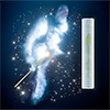
May 14, 2026 Iron-60 discovery in Antarctic ice reveals: Local Interstellar Cloud leaves its mark. (Nanowerk News) Our Solar System is currently passing through the Local Interstellar Cloud, a region of highly diluted gas and dust between the stars. On its path, Earth continuously accumulates iron-60, a rare radioactive isotope...
How particle interactions control the flow of soft materials
May 13, 2026 Using powerful X-rays and computer models, researchers inked nanoscale particle motion to surprising flow behaviors in soft materials. (Nanowerk News) Sitting in a restaurant, you reach for the ketchup bottle, eyeing the basket of fries in front of you. You give the bottle a shake, then a...
Boosting carbon capture performance with laser-engineered MOFs
May 13, 2026 Laser post-treatment tunes MOF defects and pores, boosting CO2 adsorption up to 75% while cutting costs and avoiding chemical processing. (Nanowerk News) A research team at Korea Institute of Materials Science (KIMS), led by Hee-jung Lee, senior researcher at KIMS, in collaboration with Professor Sunghwan Park of...
Galaxy cluster relaxed now, but was wild in the past

May 13, 2026 The galaxy cluster Abell 2029 is sometimes described as 'the most relaxed cluster in the Universe'. This moniker does not arise from some sort of mellow vibe, but rather because of how calm and undisturbed the superheated gas that pervades the cluster appears to be. (Nanowerk News)...
The ionic path to all-solid-state batteries
May 13, 2026 Varied particle sizes in the solid electrolyte improve ion conductivity. (Nanowerk News) All-solid-state batteries (ASSBs) are gaining traction in the energy and electric vehicle industries as potentially safer alternatives to the standard, flammable liquid batteries on the market today. However, complex challenges currently stand in the way...
Evaporation-based chip cooling recovers waste heat from high-power LEDs
May 13, 2026 Evaporation-assisted chip cooling lowers LED temperatures while preserving heat flow for small but useful waste-heat energy recovery. (Nanowerk Spotlight) A high-power chip can overheat itself into failure. Conventional chip cooling keeps devices alive by moving heat into air or coolant, where it is lost unless a larger...
Quantum geometry lens shines new light on solids

May 13, 2026 A new approach to looking at solids provides theoretical limits on some of their properties. (Nanowerk News) Two RIKEN physicists have established new theoretical limits for experimentally measurable quantities by viewing solids through a lens of quantum geometry. Their results shed light both on the physics of...
How black hole mergers are helping scientists calibrate the Universe’s most sensitive instruments
May 13, 2026 An international team of scientists has shown for the first time that gravitational waves, ripples in space and time produced by some of the most violent events in the Universe, such as the collision of two black holes, can be used to measure and correct the calibration...
Gold nanoparticles that behave like a liquid

May 13, 2026 Gold nanoparticle layers dynamically reorganize with temperature and compression, enabling tunable, responsive materials for biomedical and nanotechnology uses. (Nanowerk News) When inorganic nanoparticles come together, their optical, electronic, and magnetic properties depend strongly on how they are arranged. Being able to reorganize these arrangements in a controlled...