
Feb 02, 2026 Carbon nanotubes can open and close in response to acidity, guiding water and ions one by one and mimicking how natural cell channels work. (Nanowerk News) When water and ions move together through channels only a nanometer wide, they behave in unusual ways. In these tight spaces,...
Voltage tunable polaritonic crystals bring dynamic control to nanoscale light

Feb 02, 2026 A hybrid graphene and molybdenum trioxide crystal allows real time electrical tuning of Bloch modes and light emission, overcoming the static limits of conventional polaritonic crystals. (Nanowerk News) Polaritons are hybrid particles that form when light couples to vibrations or electrons in a material. Because they can...
Reshaping nanoporous gold leads to new electronic and optical properties
Feb 02, 2026 By changing the physical structure of gold at the nanoscale, researchers can drastically change how the material interacts with light and, as a result, its electronic and optical properties. (Nanowerk News) Gold plays a crucial role in modern advanced technology thanks to its unique properties. New research...
This chip catches AI image fakes by turning light into unforgeable watermarks

Feb 02, 2026 A semiconductor device generates unforgeable watermarks from chaotic electron behavior, embedding invisible markers in images that expose AI manipulation at the pixel level while also enabling stronger encryption. (Nanowerk Spotlight) Digital photographs can no longer be trusted as evidence. Generative artificial intelligence now swaps faces, alters expressions,...
Web-based tool visualizes catalyst gene profiles for materials design

Feb 02, 2026 A new web-based tool visualizes catalyst gene profiles, helping scientists explore patterns and improve catalyst design. (Nanowerk News) Modern industry relies heavily on catalysts, which are substances that speed up chemical reactions. They’re vital in everything from manufacturing household chemicals to generating clean energy or recycling waste....
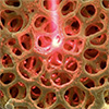
Tiny titanium pillars move hydrogen-powered flight closer to reality

Feb 01, 2026 Ultrathin titanium flow distributors made via laser micromachining achieve record fuel cell power densities, surpassing European aerospace targets set for the end of this decade. (Nanowerk Spotlight) In 2014, Toyota launched the Mirai, the world's first mass-produced hydrogen fuel cell vehicle. The car represented a genuine engineering...
Nanotechnology Now – News Story: New light-based nanotechnology could enable more precise, less harmful cancer treatment: The approach offers a potential alternative to chemotherapy and radiation by using light and heat to target cancer cells.

Home > News > New light-based nanotechnology could enable more precise, less harmful cancer treatment: The approach offers a potential alternative to chemotherapy and radiation by using light and heat to target cancer cells. January 30th, 2026 New light-based nanotechnology could enable more precise, less harmful cancer treatment: The approach...
Nanotechnology Now – Press Release: MXene nanomaterials enter a new dimension Multilayer nanomaterial: MXene flakes created at Drexel University show new promise as 1D scrolls
Home > Press > MXene nanomaterials enter a new dimension Multilayer nanomaterial: MXene flakes created at Drexel University show new promise as 1D scrolls Researchers from Drexel University have developed a process for producing 1D nanoscrolls using MXene as a precursor material. The scrolls could be used as components to...
Nanotechnology Now – Press Release: Projecting light to dispense liquids: A new route to ultra-precise microdroplets
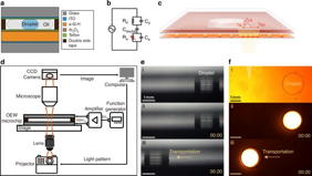
Home > Press > Projecting light to dispense liquids: A new route to ultra-precise microdroplets Overview of the OEW-based droplet dispensing system. a Schematic diagram of the microchip. b Equivalent circuit diagram of OEW. c Principle diagram of OEW. d Schematic diagram of the system. e Side view (f) Top...
Nanotechnology Now – Press Release: Breathing new life into nanotubes for a cooler planet:Researchers at Skoltech discover a simple, single-step heat treatment that nearly doubles the CO2-trapping power of carbon nanotubes
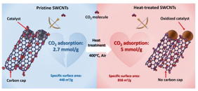
Home > Press > Breathing new life into nanotubes for a cooler planet:Researchers at Skoltech discover a simple, single-step heat treatment that nearly doubles the CO2-trapping power of carbon nanotubes Single-step thermal treatment of single-walled carbon nanotubes for enhanced CO2 adsorption capacity Credit Amit Kumar Pal, Dmitry V. Krasnikov,...