| Jun 15, 2022 |
|
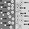
(Nanowerk News) PN junction is the elementary building block of semiconductor devices, like diode, solar cell and LED, which make up the modern (opto-)electronics.
|
|
Recently, researchers from the Shanghai Institute of Technical Physics of the Chinese Academy of Sciences have proposed a novel method to fabricate two-dimensional PN junction. This method simplifies the semiconductor manufacturing process and is well-suited to develop (opto-)electronic devices at the ultimate physical limit.
|
|
The study was published in Light: Science & Applications (“Pristine PN junction toward atomic layer devices”).
|
|
The researchers found that a number of Van der Waals materials do not need artificial doping, and they can dope themselves from n- to p- type conductance with an increasing/decreasing thickness. For example, MoTe2 material exhibits p-type, unintentional doping and n-type doping behaviors when it has one molecular layer, three molecular layers, and five molecular layer thickness, respectively.
|
|
“Using this novel property, we can easily fabricate atomically abrupt PN junctions on a variety of two-dimensional materials, which is out of the range of traditional techniques,” said XIA Hui, first author of the study.
|
|
Moreover, there are no complicated photolithography and chemical doping processes in layered junction devices. Instead, it is only the geometry of the material that is needed to be shaped.
|
|
“These findings may open a new avenue to develop novel nanodevice applications, where the geometrical size becomes the only critical factor in tuning charge-carrier distribution and functionality,” said XIA.
|
