Home > Press > Development of a diamond transistor with high hole mobility: Unconventional removal of acceptors enhanced performance
 |
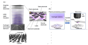
| Figure. (a) Structure of the diamond field-effect transistor (FET) fabricated in this research. The design of this FET allows Hall measurements to be performed while applying a gate voltage, enabling evaluation of the density and mobility of holes in the FET channel. (b) The surface of the diamond substrate was first exposed to hydrogen plasma to terminate it with hydrogen. The substrate was then transferred in vacuum into a glovebox filled with argon gas. Finally, cleaved single-crystalline hexagonal boron nitride (h-BN) was attached to the diamond substrate, thereby reducing the amount of airborne substancewhich act as acceptorsattaching to the diamond surface.
CREDIT Takahide Yamaguchi National Institute for Materials Science YAMAGUCHI.Takahide@nims.go.jp |
Abstract:
Using a new fabrication technique, NIMS has developed a diamond field-effect transistor (FET) with high hole mobility, which allows reduced conduction loss and higher operational speed. This new FET also exhibits normally-off behavior (i.e., electric current flow through the transistor ceases when no gate voltage is applied, a feature that makes electronic devices safer). These results may facilitate the development of low-loss power conversion and high-speed communications devices.
Development of a diamond transistor with high hole mobility: Unconventional removal of acceptors enhanced performance
Tsukuba, Japan | Posted on February 25th, 2022
Diamond has excellent wide bandgap semiconductor properties: its bandgap is larger than those of silicon carbide and gallium nitride, which are already in practical use. Diamond therefore could potentially be used to create power electronics and communications devices capable of operating more energy efficiently at higher speeds, voltages and temperatures. A number of R&D projects have previously been carried out with the aim of creating FETs using hydrogen-terminated diamonds (i.e., diamonds with their superficial carbon atoms covalently bonded with hydrogen atoms). However, these efforts have failed to fully exploit diamonds excellent wide bandgap semiconductor properties: the hole mobility (a measure of how quickly holes can move) of these diamond-integrated transistors was only 110% that of the diamonds before integration.
The NIMS research team succeeded in developing a high-performance FET by using hexagonal boron nitride (h-BN) as a gate insulator instead of conventionally used oxides (e.g., alumina), and by employing a new fabrication technique capable of preventing the surface of hydrogen-terminated diamond from being exposed to air. At high hole densities, the hole mobility of this FET was five times that of conventional FETs with oxide gate insulators. FETs with high hole mobility can operate with lower electrical resistance, thereby reducing conduction loss, and can be used to develop higher speed and smaller electronic devices. The team also demonstrated normally-off operation of the FET, an important feature for power electronics applications. The new fabrication technique enabled removal of electron acceptors from the surface of the hydrogen-terminated diamond. This was the key to the teams success in developing the high-performance FET, although these acceptors had generally been thought to be necessary in inducing electrical conductivity in hydrogen-terminated diamonds.
These results are new mileposts in the development of efficient diamond transistors for high-performance power electronics and communications devices. The team hopes to further improve the physical properties of the diamond FET and to make it more suitable for practical use.
***
This project was carried out by NIMS researchers (Yosuke Sasama, Taisuke Kageura, Masataka Imura, Kenji Watanabe, Takashi Taniguchi, Takashi Uchihashi and Takahide Yamaguchi (also an associate professor at University of Tsukuba)). This study was conducted in conjunction with other projects, including the one entitled Creation of a high-mobility field-effect transistor with a heterostructure of diamond and hexagonal boron nitride and exploration of quantum transport in it (project number: 19H02605) funded by the JSPS Grant-in-Aid for Scientific Research (B).
This research was published in Nature Electronics, an online journal, on December 23, 2021.
####
For more information, please click here
Contacts:
Yasufumi Nakamichi
National Institute for Materials Science, Japan
Office: 81-29-859-2105
Expert Contact
Takahide Yamaguchi
National Institute for Materials Science
Copyright © National Institute for Materials Science, Japan
If you have a comment, please Contact us.
Issuers of news releases, not 7th Wave, Inc. or Nanotechnology Now, are solely responsible for the accuracy of the content.
Bookmark:


News and information
![]()
More sensitive X-ray imaging: Improvements in the material that converts X-rays into light, for medical or industrial images, could allow a tenfold signal enhancement February 25th, 2022
![]()
Breaking the black box of catalytic reactions: Research offers new understanding of complex catalysis, advances catalyst design February 25th, 2022
![]()
A new platform for customizable quantum devices February 25th, 2022
![]()
Inorganic borophene liquid crystals: A superior new material for optoelectronic devices February 25th, 2022
Wireless/telecommunications/RF/Antennas/Microwaves
![]()
UMass Lowell scientist pioneers new class of semiconductors: $1.7M NSF project aims to improve wireless communication, imaging, more December 17th, 2021
![]()
Thin-film, high-frequency antenna array offers new flexibility for wireless communications November 5th, 2021
![]()
Graphene nanotubes provide a shortcut to add conductivity to powder coatings October 1st, 2021
Possible Futures
![]()
More sensitive X-ray imaging: Improvements in the material that converts X-rays into light, for medical or industrial images, could allow a tenfold signal enhancement February 25th, 2022
![]()
Breaking the black box of catalytic reactions: Research offers new understanding of complex catalysis, advances catalyst design February 25th, 2022
![]()
A new platform for customizable quantum devices February 25th, 2022
![]()
Entanglement unlocks scaling for quantum machine learning: New No-Free-Lunch theorem for quantum neural networks gives hope for quantum speedup February 25th, 2022
Chip Technology
![]()
A new platform for customizable quantum devices February 25th, 2022
![]()
Revealing new states in 2D materials February 25th, 2022
![]()
NGI advances graphene spintronics as 1D contacts improve mobility in nano-scale devices February 11th, 2022
![]()
Wise-integration and EDOM Technology Announce Channel Partnership for GaN IC Power Semiconductor Deployment February 11th, 2022
Discoveries
![]()
More sensitive X-ray imaging: Improvements in the material that converts X-rays into light, for medical or industrial images, could allow a tenfold signal enhancement February 25th, 2022
![]()
Breaking the black box of catalytic reactions: Research offers new understanding of complex catalysis, advances catalyst design February 25th, 2022
![]()
A new platform for customizable quantum devices February 25th, 2022
![]()
Inorganic borophene liquid crystals: A superior new material for optoelectronic devices February 25th, 2022
Announcements
![]()
Workhorse of photovoltaics combined with perovskite in tandem for the first time February 25th, 2022
![]()
Shape memory in hierarchical networks the astonishing property that allows manipulation of morphing materials with micro scale resolutions February 25th, 2022
![]()
Inorganic borophene liquid crystals: A superior new material for optoelectronic devices February 25th, 2022
![]()
Revealing new states in 2D materials February 25th, 2022
Interviews/Book Reviews/Essays/Reports/Podcasts/Journals/White papers/Posters
![]()
Cutting through the noise: Berkeley Lab error mitigation approach helps quantum computers level up February 25th, 2022
![]()
Workhorse of photovoltaics combined with perovskite in tandem for the first time February 25th, 2022
![]()
Shape memory in hierarchical networks the astonishing property that allows manipulation of morphing materials with micro scale resolutions February 25th, 2022
![]()
Inorganic borophene liquid crystals: A superior new material for optoelectronic devices February 25th, 2022