Home > Press > Drawing data in nanometer scale
 |
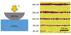
| Left: Data storage using probe force. Right: Data storage area drawn with a width of 10 nm or less.
CREDIT POSTECH |
Abstract:
Frank Holzenburg, an artist with tens of thousands of followers across his social networking accounts, has attracted attention for his life-like drawings that are smaller than a fingernail. Recently, a method to draw data in an area smaller than 10 nanometers (nm; 1 nm = 1 billionth of a meter) like drawing a small picture on paper has been proposed.
Drawing data in nanometer scale
Pohang, Korea | Posted on September 30th, 2022
A joint research team led by Professor Daesu Lee (Department of Physics) of POSTECH, Professor Se Young Park (Department of Physics) at Soongsil University, and Dr. Ji Hye Lee (Department of Physics and Astronomy) of Seoul National University has proposed a method for densely storing data by poking with a sharp probe. This method utilizes a material in the metastable state, whose properties change easily even with slight stimulation.
A thin film of metastable ferroelectric calcium titanate (CaTiO3) enables the polarization switching of a material even with a slight pressure of a probe: A very weak force of 100 nanonewtons (nN) is more than enough. The joint research team succeeded in making the width of the polarization path smaller than 10 nm by using this force and found the way to dramatically increase the capacity of data storage. This is because the smaller the size of the path, the more data the single material can store.
The data storage capacity increased by up to 1 terabit (Tbit)/cm as a result of drawing the data storage area using a probe on the thin film. This result is 10 times greater than that of a previous study (0.11Tbit/cm²) which suggested a probe-based storage method using another material. Unlike the data storage method that uses electric fields, this probe method only requires a very small force, so the burden on the device is also small.
The results from the study are drawing attention as they have proved that materials achieve higher performance in an unstable metastable state. The findings are anticipated to be applicable in the next-generation electronic devices with improved integration and efficiency in the future.
Recently published in Physical Review Letters, one of the most authoritative journals in the field of physics, this study was supported by the Institute for Basic Science, and by the Research Center Program, the Basic Science Research Institute Fund, and the Key Research Institutes in Universities program of the National Research Foundation of Korea.
####
For more information, please click here
Contacts:
Jinyoung Huh
Pohang University of Science & Technology (POSTECH)
Office: 82-54-279-2415
Copyright © Pohang University of Science & Technology (POSTECH)
If you have a comment, please Contact us.
Issuers of news releases, not 7th Wave, Inc. or Nanotechnology Now, are solely responsible for the accuracy of the content.
News and information
![]()
Researchers unveil mystery inside Li- o2 batteries September 30th, 2022
![]()
Synthesis of air-stable room-temperature van der Waals magnetic thin flakes September 30th, 2022
Govt.-Legislation/Regulation/Funding/Policy
![]()
Solvent study solves solar cell durability puzzle: Rice-led project could make perovskite cells ready for prime time September 23rd, 2022
![]()
Heat-resistant nanophotonic material could help turn heat into electricity: The key to beating the heat is degrading the materials in advance September 23rd, 2022
![]()
Reduced power consumption in semiconductor devices September 23rd, 2022
Possible Futures
![]()
Researchers unveil mystery inside Li- o2 batteries September 30th, 2022
![]()
Synthesis of air-stable room-temperature van der Waals magnetic thin flakes September 30th, 2022
![]()
Layer Hall effect and hidden Berry curvature in antiferromagnetic insulators September 30th, 2022
Announcements
![]()
Researchers unveil mystery inside Li- o2 batteries September 30th, 2022
![]()
Synthesis of air-stable room-temperature van der Waals magnetic thin flakes September 30th, 2022
![]()
Layer Hall effect and hidden Berry curvature in antiferromagnetic insulators September 30th, 2022
Interviews/Book Reviews/Essays/Reports/Podcasts/Journals/White papers/Posters
![]()
Conformal optical black hole for cavity September 30th, 2022
![]()
Ultrasmall VN/Co heterostructure with optimized N active sites anchored in N-doped graphitic nanocarbons for boosting hydrogen evolution September 30th, 2022
![]()
Layer Hall effect and hidden Berry curvature in antiferromagnetic insulators September 30th, 2022
Human Interest/Art
![]()
Scientists prepare for the worlds smallest race: Nanocar Race II March 18th, 2022
![]()
Graphene nanotubes revolutionize touch screen use for prosthetic hands August 3rd, 2021
![]()
JEOL Announces 2020 Microscopy Image Grand Prize Winners January 7th, 2021
Grants/Sponsored Research/Awards/Scholarships/Gifts/Contests/Honors/Records
![]()
Multi-institution, $4.6 million NSF grant to fund nanotechnology training September 9th, 2022
![]()
Understanding outsize role of nanopores: New research reveals differences in pH, and more, about these previously mysterious environments August 26th, 2022
![]()
New chip ramps up AI computing efficiency August 19th, 2022


