Home > Press > On-chip single-mode CdS nanowire laser
 |
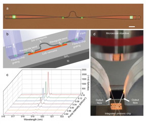
| a, optical image of a hybrid MZI structure under excitation. b, the schematic configuration of the on-chip nanowire laser. A CdS nanowire is used as the gain material and is evanescently coupled to an ?-shaped SiN waveguide at both sides to form a hybrid MZI structure. In the coupling area, SiN waveguide bends are predesigned to ensure a high coupling efficiency with excellent reproducibility. Fibre-to-chip grating couplers are designed at both ends of the SiN waveguide, which couple the laser signal from the on-chip SiN waveguide into standard optical fibres for optical characterization. c, Lasing spectra obtained at different pumping intensities above the threshold. The dominant lasing peak is centered at a wavelength of approximately 518.9 nm with a linewidth of approximately 0.1 nm. The side-mode suppression ratio increases with increasing pumping intensity and realizes a maximum value of approximately a factor of 20 (13 dB). d, optical image of the measurement setup under an optical microscope. The measurement setup uses output fibres to collect signals out of the chip via fibre-to-chip grating couplers.
CREDIT by Qingyang Bao, Weijia Li, Peizhen Xu, Ming Zhang, Daoxin Dai, Pan Wang, Xin Guo, and Limin Tong |
Abstract:
In the past decade, on-chip nanophotonics has attracted increasing attention for the realization of integrated photonic circuits with faster operation, broader bandwidth, lower power consumption and higher compactness. While a number of on-chip nanophotonic devices and circuits have been successfully fabricated using a complementary metal-oxide semiconductor (CMOS) -compatible technique, on-chip light sources remain challenging. On the other hand, bottom-up grown semiconductor nanowires have long been used for nanoscale waveguide lasers. In recent years, increasing attention has been paid to the integration of active nanowires with on-chip planar waveguides for on-chip light sources. However, due to the large discrepancy in fabrication techniques, refractive index and geometric compatibility between a freestanding nanowire and an on-chip planar waveguide, a variety of issues, including a relatively low coupling efficiency, ineffective mode selection and low reproductivity, have yet to be addressed.
On-chip single-mode CdS nanowire laser
Changchun, China | Posted on March 21st, 2020
In a new paper published in Light Science & Application, scientists from the State Key Laboratory of Modern Optical Instrumentation, College of Optical Science and Engineering, Zhejiang University, China demonstrated an on-chip single-mode CdS nanowire laser with high coupling efficiency. The mode selection is realized using a Mach-Zehnder interferometer (MZI) structure. When the pumping intensity exceeds the lasing threshold of 4.9 kW/cm2, on-chip single-mode lasing at approximately 518.9 nm is achieved with a linewidth of 0.1 nm and a side-mode suppression ratio of 20 (13 dB). The output of the nanowire laser is channelled into an on-chip SiN waveguide with high efficiency (up to 58%) by evanescent coupling, and the directional coupling ratio between the two output ports can be varied from 90% to 10% by predesigning the coupling length of the SiN waveguide. Benefitting from the great diversity of the available nanowire materials and high flexibility for bandgap engineering, the on-chip integration scheme demonstrated here can be readily extended to realize on-chip nanolasers from the ultraviolet to near-infrared ranges, which may offer new opportunities for both semiconductor nanowires and on-chip photonic devices.
These scientists summarize the fabrication and operational principle of the laser:
“We use micromanipulation under an optical microscope to integrate a CdS nanowire onto a SiN chip and form a hybrid MZI structure with excellent reproducibility. By using the MZI for mode selection, we operate the laser in single mode. We can also change the output ratios between the two ports of the lasing MZI by using different coupling lengths of the waveguide bends.”
“The overall size of the hybrid MZI structure is kept below 100 μm. Fibre-to-chip grating couplers are designed at both ends of the SiN waveguide, which couple the laser signal from the on-chip SiN waveguide into standard optical fibres for optical characterization.” “By comparing the lasing output intensities from the nanowire end and the grating area, we estimate the fractional power channelled into the SiN waveguide to be approximately 58%, much higher than previous results obtained in chip integrated nanowire lasers, and can be further improved by optimizing the coupling efficiency between the nanowire and the SiN waveguide.” they added.
“Benefitting from the great diversity of the available nanowire materials and high flexibility for bandgap engineering, the on-chip integration scheme demonstrated here can be readily extended to realize on-chip nanolasers from the ultraviolet to near-infrared ranges, and the on-chip single-mode nanowire laser may thus offer an opportunity to develop on-chip physical and biochemical optical sensors with higher stability and compactness. ” the scientists forecast.
####
For more information, please click here
Contacts:
Xin Guo
Copyright © Changchun Institute of Optics, Fine Mechanics and Physics, Chinese Academy of Sciences
If you have a comment, please Contact us.
Issuers of news releases, not 7th Wave, Inc. or Nanotechnology Now, are solely responsible for the accuracy of the content.
Bookmark:


News and information
![]() Quantum phenomenon governs organic solar cells: Vibronic coherence contributes to photocurrent generation in organic semiconductor heterojunction diodes March 30th, 2020
Quantum phenomenon governs organic solar cells: Vibronic coherence contributes to photocurrent generation in organic semiconductor heterojunction diodes March 30th, 2020
![]() Double-walled nanotubes have electro-optical advantages :Rice University calculations show they could be highly useful for solar panels March 27th, 2020
Double-walled nanotubes have electro-optical advantages :Rice University calculations show they could be highly useful for solar panels March 27th, 2020
![]() Artificial intelligence identifies optimal material formula March 26th, 2020
Artificial intelligence identifies optimal material formula March 26th, 2020
![]() Light in the tunnel March 26th, 2020
Light in the tunnel March 26th, 2020
Govt.-Legislation/Regulation/Funding/Policy
![]() Double-walled nanotubes have electro-optical advantages :Rice University calculations show they could be highly useful for solar panels March 27th, 2020
Double-walled nanotubes have electro-optical advantages :Rice University calculations show they could be highly useful for solar panels March 27th, 2020
![]() Electric jolt to carbon makes better water purifier March 24th, 2020
Electric jolt to carbon makes better water purifier March 24th, 2020
![]() Heterostructure and Q-factor engineering for low-threshold and persistent nanowire lasing March 22nd, 2020
Heterostructure and Q-factor engineering for low-threshold and persistent nanowire lasing March 22nd, 2020
![]() New mechanism of optical gain in two-dimensional material requires only extremely low input power March 20th, 2020
New mechanism of optical gain in two-dimensional material requires only extremely low input power March 20th, 2020
Possible Futures
![]() Quantum phenomenon governs organic solar cells: Vibronic coherence contributes to photocurrent generation in organic semiconductor heterojunction diodes March 30th, 2020
Quantum phenomenon governs organic solar cells: Vibronic coherence contributes to photocurrent generation in organic semiconductor heterojunction diodes March 30th, 2020
![]() Double-walled nanotubes have electro-optical advantages :Rice University calculations show they could be highly useful for solar panels March 27th, 2020
Double-walled nanotubes have electro-optical advantages :Rice University calculations show they could be highly useful for solar panels March 27th, 2020
![]() Artificial intelligence identifies optimal material formula March 26th, 2020
Artificial intelligence identifies optimal material formula March 26th, 2020
![]() Light in the tunnel March 26th, 2020
Light in the tunnel March 26th, 2020
Chip Technology
![]() Double-walled nanotubes have electro-optical advantages :Rice University calculations show they could be highly useful for solar panels March 27th, 2020
Double-walled nanotubes have electro-optical advantages :Rice University calculations show they could be highly useful for solar panels March 27th, 2020
![]() Light in the tunnel March 26th, 2020
Light in the tunnel March 26th, 2020
![]() Heterostructure and Q-factor engineering for low-threshold and persistent nanowire lasing March 22nd, 2020
Heterostructure and Q-factor engineering for low-threshold and persistent nanowire lasing March 22nd, 2020
![]() New mechanism of optical gain in two-dimensional material requires only extremely low input power March 20th, 2020
New mechanism of optical gain in two-dimensional material requires only extremely low input power March 20th, 2020
Sensors
![]() Tokai scientists create the world’s first electronic skin-based sensor for heatstroke detection March 17th, 2020
Tokai scientists create the world’s first electronic skin-based sensor for heatstroke detection March 17th, 2020
![]() Better biosensor technology created for stem cells: Rutgers innovation may help guide treatment of Alzheimer’s, Parkinson’s diseases November 12th, 2019
Better biosensor technology created for stem cells: Rutgers innovation may help guide treatment of Alzheimer’s, Parkinson’s diseases November 12th, 2019
Discoveries
![]() Quantum phenomenon governs organic solar cells: Vibronic coherence contributes to photocurrent generation in organic semiconductor heterojunction diodes March 30th, 2020
Quantum phenomenon governs organic solar cells: Vibronic coherence contributes to photocurrent generation in organic semiconductor heterojunction diodes March 30th, 2020
![]() Double-walled nanotubes have electro-optical advantages :Rice University calculations show they could be highly useful for solar panels March 27th, 2020
Double-walled nanotubes have electro-optical advantages :Rice University calculations show they could be highly useful for solar panels March 27th, 2020
![]() Artificial intelligence identifies optimal material formula March 26th, 2020
Artificial intelligence identifies optimal material formula March 26th, 2020
![]() Light in the tunnel March 26th, 2020
Light in the tunnel March 26th, 2020
Announcements
![]() Quantum phenomenon governs organic solar cells: Vibronic coherence contributes to photocurrent generation in organic semiconductor heterojunction diodes March 30th, 2020
Quantum phenomenon governs organic solar cells: Vibronic coherence contributes to photocurrent generation in organic semiconductor heterojunction diodes March 30th, 2020
![]() Double-walled nanotubes have electro-optical advantages :Rice University calculations show they could be highly useful for solar panels March 27th, 2020
Double-walled nanotubes have electro-optical advantages :Rice University calculations show they could be highly useful for solar panels March 27th, 2020
![]() Artificial intelligence identifies optimal material formula March 26th, 2020
Artificial intelligence identifies optimal material formula March 26th, 2020
![]() Light in the tunnel March 26th, 2020
Light in the tunnel March 26th, 2020
Interviews/Book Reviews/Essays/Reports/Podcasts/Journals/White papers/Posters
![]() Quantum phenomenon governs organic solar cells: Vibronic coherence contributes to photocurrent generation in organic semiconductor heterojunction diodes March 30th, 2020
Quantum phenomenon governs organic solar cells: Vibronic coherence contributes to photocurrent generation in organic semiconductor heterojunction diodes March 30th, 2020
![]() Double-walled nanotubes have electro-optical advantages :Rice University calculations show they could be highly useful for solar panels March 27th, 2020
Double-walled nanotubes have electro-optical advantages :Rice University calculations show they could be highly useful for solar panels March 27th, 2020
![]() Artificial intelligence identifies optimal material formula March 26th, 2020
Artificial intelligence identifies optimal material formula March 26th, 2020
![]() Light in the tunnel March 26th, 2020
Light in the tunnel March 26th, 2020
Photonics/Optics/Lasers
![]() Light in the tunnel March 26th, 2020
Light in the tunnel March 26th, 2020
![]() Heterostructure and Q-factor engineering for low-threshold and persistent nanowire lasing March 22nd, 2020
Heterostructure and Q-factor engineering for low-threshold and persistent nanowire lasing March 22nd, 2020
![]() O-FIB: Far-field-induced near-field breakdown for direct nanowriting in an atmospheric environment March 20th, 2020
O-FIB: Far-field-induced near-field breakdown for direct nanowriting in an atmospheric environment March 20th, 2020
![]() New mechanism of optical gain in two-dimensional material requires only extremely low input power March 20th, 2020
New mechanism of optical gain in two-dimensional material requires only extremely low input power March 20th, 2020