
Home > Press > Optical vacuum cleaner can manipulate nanoparticles: The TPU and international researchers developed a concept for constructing an optical vacuum cleaner; due to its optical properties, it can trap nanoparticles from the environment; currently, there are no sufficiently effective
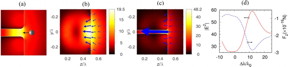 |
| (a) Schematic diagram for the “optical vacuum cleaner”, where a nanoparticle is pulled by the optical force, and moves towards the nanohole structured dielectric cuboid. (b,c) Light intensity (|E|2) and optical force distributions for (b) solid cuboid without a hole, (c) cuboid with a 20?nm hole. The refractive index and size of the simulated cuboids are set to be n?=?2 and L?=?λ. (d) Optical force and light intensity vs illumination wavelength, at the opening of the nanohole. The optical force is assumed to be exerted on a gold nanosphere with the radius of d?=?15?nm and complex dielectric permittivity εp?=??9.421?+?1.504 i at λ?=?600?nm35, and calculated using the dipole approximation. The arrows in blue color represent the optical gradient force.
CREDIT Tomsk Polytechnic University |
Abstract:
Scientists of Tomsk Polytechnic University jointly with Russian and international colleagues developed the concept for constructing an “optical vacuum cleaner”. Due to its optical properties, it can trap nanoparticles from the environment. Currently, there are no effective devices for this task. The research results were published in Scientific Reports (IF:4,525; Q1). In the future, such “vacuum cleaners” can be utilized for air purification during lab-on-a-chip operations and preparation of clean rooms.
Optical vacuum cleaner can manipulate nanoparticles: The TPU and international researchers developed a concept for constructing an optical vacuum cleaner; due to its optical properties, it can trap nanoparticles from the environment; currently, there are no sufficiently effective
Tomsk, Russia | Posted on September 13th, 2019
“The size of nanoparticles varies from 1 to a maximum of 100 nanometers. Currently, researchers from all around the world are seeking for the ways to control such small particles and manipulate them for various applications. However, there have been no sufficiently effective and widely used devices for such tasks yet. We offer a new concept for particle manipulation and capture – it is “optical vacuum cleaner” – says Oleg Minin, Professor of the TPU Division for Electronic Engineering.
According to this concept, an “optical vacuum cleaner” is a dielectric microparticle. In the published article, the scientists used particles having the shape of an equilateral cuboid. The particles have a nanoscale gouge or nanohole. When they are exposed to optical radiation, such as laser, there is optical pressure.
“The resultant force is directed inside our cuboid, trapping nanoparticles into the hole. The ?apacity, respectively, depends on the size of the hole”, – says the scientist.
This concept can be implemented in the so-called lab-on-a-chip work in biomedical research. This technique can combine several laboratory functions on a chip, varying in size from a few square millimeters to square centimeters. This advanced on-chip analysis method will allow achieving high-throughput screening and automation. Cleaning chip surface and ambient air from foreign nanoparticles will allow increasing the analyzes sensitivity and the result accuracy.
The study was conduct by Russian and international specialists from Jilin University (China) and Ben-Gurion University (Israel). The next stage will be experimental confirmation of the concept.
####
For more information, please click here
Contacts:
Vitalii Sdelnikov
7-382-260-6404
Copyright © Tomsk Polytechnic University
If you have a comment, please Contact us.
Issuers of news releases, not 7th Wave, Inc. or Nanotechnology Now, are solely responsible for the accuracy of the content.
Bookmark:


News and information
![]() A Quantum Leap: $25M grant makes UC Santa Barbara home to the nations first NSF-funded Quantum Foundry, a center for development of materials for quantum information-based technologies September 16th, 2019
A Quantum Leap: $25M grant makes UC Santa Barbara home to the nations first NSF-funded Quantum Foundry, a center for development of materials for quantum information-based technologies September 16th, 2019
![]() Journal Nanotechnology Progress International (JONPI), volume 7, issue 1 out September 16th, 2019
Journal Nanotechnology Progress International (JONPI), volume 7, issue 1 out September 16th, 2019
![]() MIT engineers develop ‘blackest black’ material to date: Made from carbon nanotubes, the new coating is 10 times darker than other very black materials September 13th, 2019
MIT engineers develop ‘blackest black’ material to date: Made from carbon nanotubes, the new coating is 10 times darker than other very black materials September 13th, 2019
Lab-on-a-chip
![]() Dynamic hydrogel used to make ‘soft robot’ components and LEGO-like building blocks March 22nd, 2019
Dynamic hydrogel used to make ‘soft robot’ components and LEGO-like building blocks March 22nd, 2019
![]() Researchers make flexible glass for tiny medical devices: Glass can bend over and over again on a nanoscale March 27th, 2017
Researchers make flexible glass for tiny medical devices: Glass can bend over and over again on a nanoscale March 27th, 2017
Possible Futures
![]() A Quantum Leap: $25M grant makes UC Santa Barbara home to the nations first NSF-funded Quantum Foundry, a center for development of materials for quantum information-based technologies September 16th, 2019
A Quantum Leap: $25M grant makes UC Santa Barbara home to the nations first NSF-funded Quantum Foundry, a center for development of materials for quantum information-based technologies September 16th, 2019
![]() New health monitors are flexible, transparent and graphene enabled September 13th, 2019
New health monitors are flexible, transparent and graphene enabled September 13th, 2019
![]() One-atom switch supercharges fluorescent dyes: Rice University lab discovers simple technique to make biocompatible ‘turn-on’ dyes September 13th, 2019
One-atom switch supercharges fluorescent dyes: Rice University lab discovers simple technique to make biocompatible ‘turn-on’ dyes September 13th, 2019
Chip Technology
![]() A Quantum Leap: $25M grant makes UC Santa Barbara home to the nations first NSF-funded Quantum Foundry, a center for development of materials for quantum information-based technologies September 16th, 2019
A Quantum Leap: $25M grant makes UC Santa Barbara home to the nations first NSF-funded Quantum Foundry, a center for development of materials for quantum information-based technologies September 16th, 2019
![]() Measuring changes in magnetic order to find ways to transcend conventional electronics September 6th, 2019
Measuring changes in magnetic order to find ways to transcend conventional electronics September 6th, 2019
Nanoelectronics
![]() Beyond 1 and 0: Engineers boost potential for creating successor to shrinking transistors May 30th, 2019
Beyond 1 and 0: Engineers boost potential for creating successor to shrinking transistors May 30th, 2019
Discoveries
![]() New health monitors are flexible, transparent and graphene enabled September 13th, 2019
New health monitors are flexible, transparent and graphene enabled September 13th, 2019
![]() One-atom switch supercharges fluorescent dyes: Rice University lab discovers simple technique to make biocompatible ‘turn-on’ dyes September 13th, 2019
One-atom switch supercharges fluorescent dyes: Rice University lab discovers simple technique to make biocompatible ‘turn-on’ dyes September 13th, 2019
Announcements
![]() Journal Nanotechnology Progress International (JONPI), volume 7, issue 1 out September 16th, 2019
Journal Nanotechnology Progress International (JONPI), volume 7, issue 1 out September 16th, 2019
![]() MIT engineers develop ‘blackest black’ material to date: Made from carbon nanotubes, the new coating is 10 times darker than other very black materials September 13th, 2019
MIT engineers develop ‘blackest black’ material to date: Made from carbon nanotubes, the new coating is 10 times darker than other very black materials September 13th, 2019
![]() Inspired by natural signals in living cells, researchers design artificial gas detector: Tiny box puts itself together and glows September 13th, 2019
Inspired by natural signals in living cells, researchers design artificial gas detector: Tiny box puts itself together and glows September 13th, 2019
Interviews/Book Reviews/Essays/Reports/Podcasts/Journals/White papers
![]() Journal Nanotechnology Progress International (JONPI), volume 7, issue 1 out September 16th, 2019
Journal Nanotechnology Progress International (JONPI), volume 7, issue 1 out September 16th, 2019
![]() New health monitors are flexible, transparent and graphene enabled September 13th, 2019
New health monitors are flexible, transparent and graphene enabled September 13th, 2019
![]() One-atom switch supercharges fluorescent dyes: Rice University lab discovers simple technique to make biocompatible ‘turn-on’ dyes September 13th, 2019
One-atom switch supercharges fluorescent dyes: Rice University lab discovers simple technique to make biocompatible ‘turn-on’ dyes September 13th, 2019
Tools
![]() Measuring changes in magnetic order to find ways to transcend conventional electronics September 6th, 2019
Measuring changes in magnetic order to find ways to transcend conventional electronics September 6th, 2019
![]() Save time using maths: Analytical tool designs corkscrew-shaped nano-antennae August 23rd, 2019
Save time using maths: Analytical tool designs corkscrew-shaped nano-antennae August 23rd, 2019
Photonics/Optics/Lasers
![]() Save time using maths: Analytical tool designs corkscrew-shaped nano-antennae August 23rd, 2019
Save time using maths: Analytical tool designs corkscrew-shaped nano-antennae August 23rd, 2019