Home > Press > Shape memory in hierarchical networks the astonishing property that allows manipulation of morphing materials with micro scale resolutions
 |
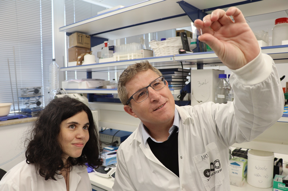
| (Left to right): Shiran Ziv Sharabani & Dr. Amit Sitt
CREDIT Tel Aviv University |
Abstract:
Researchers from Tel Aviv University have discovered, for the first time, a series of physical properties existing in polymer microfiber networks, among them shape memory. These discoveries open the doors to a range of technological and biological applications, from tissue engineering to robotics.
Shape memory in hierarchical networks the astonishing property that allows manipulation of morphing materials with micro scale resolutions
Tel-Aviv, Israel | Posted on February 25th, 2022
The study was led by Dr. Amit Sitt and doctoral student Shiran Ziv Sharabani of the Raymond and Beverly Sackler School of Chemistry and the Roman Abramovich Center for Nanoscience and Nanotechnology. The study was published in the prestigious journal Advanced Functional Materials.
Dr. Sitt explains: In the study, we created two-dimensional polymer microfiber networks which undergo temperature-induced shape changes. We discovered for the first time that such responsive sparse networks exhibit shape memory properties an especially astonishing property that we were not expecting considering their sparseness. The networks, composed of temperature-responsive polymer fibers, are controlled by the physical properties of each fiber. When these conditions are modified, the networks tend to demonstrate one of two behavior pathways upon cooling in one pathway, the fibers remain straight and the network maintains its orderly morphology, and in the other pathway the fibers bend and the network becomes tangled just like spaghetti. The beauty is that both of these behavioral pathways demonstrate shape memory, and once heated, the network resumes its original ordered morphology. This principle, which is demonstrated on various types of networks, offers a new way to control alterations in the shape of materials; and apparently even minor changes in the structure of the fibers translate into a dramatic change in the microscopic behavior of the networks.
The two-dimensional networks that were developed and manufactured at Dr. Sitts laboratory are based on a polymer called PNIPAAm, and are fabricated in a process known as “Dry Spinning”. In this process, the fibers are drawn out of the liquid polymer solution, in the course of which they rapidly harden and solidify, while rapid evaporation of the solvent leaves the polymer as a thin fiber. This method allows the creation of fibers with a thickness of a hundredth of a hairbreadth and their spatial arrangement in an orderly manner, much like three-dimensional printing, but in much smaller scales.
Dr. Sitt adds: One of the main ways in which biological systems form movements and generate forces is by the exploitation of active hierarchical networks that consist of thin micro-filaments, which can change their shape and size according to external stimuli. Such networks exist at the single cell level and take part in a range of cellular and physical processes. For example, the muscles in the human body are based on networks of protein fibers, which contract and relax following neural stimulation. While using a significantly different mechanism, our purely synthetic systems mimic this behavior, and we can now modify their response, paving the path for designing the morphing behavior of the material with microscale resolution.
Dr. Sitt and his team have explained their interesting results using a simple computational model. Doctoral student Shiran Ziv Sharabani elaborates: Our theoretical model is based on a basic understanding of spring systems, which are familiar, classic systems. We were able to describe the two behavior pathways that we observed in the laboratory using two parameters of the spring system, and this model helped us show unequivocally that a networks microscopic properties are closely related to a range of geometrical factors, chiefly the fiber diameter but also the density of the entire network.
As to the applications of polymer networks, adds Dr. Sitt, one can soar into the realms of science fiction, but at the practical level and in the near future, we are planning to use networks to make fabrics and three-dimensional structures that will change shape at the micron resolution level, in a manner that will actually be programmed into the structure of the material itself. At the same time, we are working on the use of shape-morphing networks to develop tiny artificial muscles that will be able to change the focus of soft lenses, separate nano- and micro-particles and manipulate tiny pincers for taking a biopsy of individual cells.
Ziv Sharabani concludes, saying: Using the insights of our research, one can analyze and deduce which toolbox is needed for such developments. The study, which took more than three years, included the participation of Prof. Eli Flaxer of Afeka Engineering Academic College in Tel Aviv, students, research students and a high school student. There is no doubt that the knowledge that we have acquired in the course of the research is innovative and has abundant technological potential.
####
For more information, please click here
Contacts:
Noga Shahar
Tel-Aviv University
Office: 972-547-705-223
Copyright © Tel-Aviv University
If you have a comment, please Contact us.
Issuers of news releases, not 7th Wave, Inc. or Nanotechnology Now, are solely responsible for the accuracy of the content.
Bookmark:


News and information
![]()
More sensitive X-ray imaging: Improvements in the material that converts X-rays into light, for medical or industrial images, could allow a tenfold signal enhancement February 25th, 2022
![]()
Breaking the black box of catalytic reactions: Research offers new understanding of complex catalysis, advances catalyst design February 25th, 2022
![]()
A new platform for customizable quantum devices February 25th, 2022
![]()
Inorganic borophene liquid crystals: A superior new material for optoelectronic devices February 25th, 2022
Robotics
![]()
Leibniz Prize winner Professor Dr. Oliver G. Schmidt moves to Chemnitz University of Technology: President Professor Dr. Gerd Strohmeier refers to an ‘absolute top transfer’ September 10th, 2021
![]()
Actuator discovery outperforms existing technology: University of Houston researchers use organic semiconductor nanotubes to create new electrochemical actuator September 3rd, 2021
Possible Futures
![]()
More sensitive X-ray imaging: Improvements in the material that converts X-rays into light, for medical or industrial images, could allow a tenfold signal enhancement February 25th, 2022
![]()
Breaking the black box of catalytic reactions: Research offers new understanding of complex catalysis, advances catalyst design February 25th, 2022
![]()
A new platform for customizable quantum devices February 25th, 2022
![]()
Entanglement unlocks scaling for quantum machine learning: New No-Free-Lunch theorem for quantum neural networks gives hope for quantum speedup February 25th, 2022
Nanomedicine
![]()
More sensitive X-ray imaging: Improvements in the material that converts X-rays into light, for medical or industrial images, could allow a tenfold signal enhancement February 25th, 2022
![]()
Breaking the black box of catalytic reactions: Research offers new understanding of complex catalysis, advances catalyst design February 25th, 2022
![]()
Scientists use DNA to assemble complex nanomaterials: Researchers create DNA nano-chambers with bonds that can control the assembly of targeted nanoparticle structures February 11th, 2022
Discoveries
![]()
More sensitive X-ray imaging: Improvements in the material that converts X-rays into light, for medical or industrial images, could allow a tenfold signal enhancement February 25th, 2022
![]()
Breaking the black box of catalytic reactions: Research offers new understanding of complex catalysis, advances catalyst design February 25th, 2022
![]()
A new platform for customizable quantum devices February 25th, 2022
![]()
Inorganic borophene liquid crystals: A superior new material for optoelectronic devices February 25th, 2022
Announcements
![]()
Development of a diamond transistor with high hole mobility: Unconventional removal of acceptors enhanced performance February 25th, 2022
![]()
Workhorse of photovoltaics combined with perovskite in tandem for the first time February 25th, 2022
![]()
Inorganic borophene liquid crystals: A superior new material for optoelectronic devices February 25th, 2022
![]()
Revealing new states in 2D materials February 25th, 2022
Interviews/Book Reviews/Essays/Reports/Podcasts/Journals/White papers/Posters
![]()
Cutting through the noise: Berkeley Lab error mitigation approach helps quantum computers level up February 25th, 2022
![]()
Development of a diamond transistor with high hole mobility: Unconventional removal of acceptors enhanced performance February 25th, 2022
![]()
Workhorse of photovoltaics combined with perovskite in tandem for the first time February 25th, 2022
![]()
Inorganic borophene liquid crystals: A superior new material for optoelectronic devices February 25th, 2022