Home > Press > Thermal impact of 3D stacking photonic and electronic chips: Researchers investigate how the thermal penalty of 3D integration can be minimized
 |
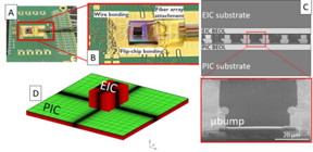
| Hybrid, 3D integrated optical transceiver. (A,B) The test setup: the photonic chip (PIC) is placed on a circuit board (green), and the electronic chip (EIC) is bonded on top of the photonic chip. (C) is a cross-section of the EIC-PIC assembly with µbumps. (D) Shows the mesh of the finite element model.
CREDIT The Authors, doi: 10.1117/1.JOM.4.1.011004. |
Abstract:
Recent advancements in AI and more specifically large language models such as ChatGPT have put a strain on data centers. AI models require huge amounts of data to train, and in order to move data between the processing units and memory, efficient communication links become necessary. For long distance communication, fiber optics has already been the go-to solution for decades. For short distance intra-data center communication, the industry is now also starting to adopt fiber optics due to its great performance compared to classical electrical links. Recent technological developments now even enable the switch from electrical to optical interconnect for very small distances, such as the communication between chips inside the same package.
Thermal impact of 3D stacking photonic and electronic chips: Researchers investigate how the thermal penalty of 3D integration can be minimized
Bellingham, WA | Posted on December 8th, 2023
This requires a conversion of the data stream from the electrical to the optical domain, which happens in the optical transceiver. Silicon photonics is the most widely used technology for fabricating these optical transceivers. The active photonic devices inside the chip (modulators and photodetectors) still require a connection with electronic drivers for powering the devices and reading the incoming data. Stacking the electronic chip (EIC) right on top of the photonic chip (PIC) by means of 3D stacking technology realizes a very tight integration of the components with low parasitic capacitance.
In research recently published in the Journal of Optical Microsystems, the thermal impact of this 3D integration is investigated. The design of the photonic chip consists of an array of ring modulators, which are known for their temperature sensitivity. In order to operate in a demanding environment, such as a data center, they need active thermal stabilization. This is implemented in the form of integrated heaters. For energy efficiency reasons, it is obvious that the power required for thermal stabilization should be minimized.
The research team from KU Leuven and imec in Belgium measured the heater efficiency of the ring modulators experimentally before and after flip-chip bonding of the EIC on the PIC. A relative loss of -43.3% in efficiency was found, which is a significant impact. Furthermore, 3D finite element simulations attributed this loss to heat spreading in the EIC. This heat spreading should be avoided, because in the ideal case all heat that is generated in the integrated heater is contained close to the photonic device. The thermal crosstalk between the photonic devices also increased by up to +44.4% after bonding the EIC, which complicates the individual thermal control.
Quantifying the thermal impact of 3D photonic-electronic integration is important, but so is the prevention of heater efficiency loss. For this reason, a thermal simulation study was conducted where typical design variables were changed with the goal of increasing the heater efficiency. It is shown that by increasing the spacing between µbumps and the photonic device, and by decreasing the interconnect linewidth, the thermal penalty of 3D integration can be minimized.
####
For more information, please click here
Contacts:
Daneet Steffens
SPIE–International Society for Optics and Photonics
Office: 360-685-5478
Copyright © SPIE–International Society for Optics and Photonics
If you have a comment, please Contact us.
Issuers of news releases, not 7th Wave, Inc. or Nanotechnology Now, are solely responsible for the accuracy of the content.
News and information
![]()
Worlds first logical quantum processor: Key step toward reliable quantum computing December 8th, 2023
![]()
VUB team develops breakthrough nanobody technology against liver inflammation December 8th, 2023
![]()
Finding the most heat-resistant substances ever made: UVA Engineering secures DOD MURI award to advance high-temperature materials December 8th, 2023
Possible Futures
![]()
Worlds first logical quantum processor: Key step toward reliable quantum computing December 8th, 2023
![]()
VUB team develops breakthrough nanobody technology against liver inflammation December 8th, 2023
![]()
Finding the most heat-resistant substances ever made: UVA Engineering secures DOD MURI award to advance high-temperature materials December 8th, 2023
Chip Technology
![]()
2D material reshapes 3D electronics for AI hardware December 8th, 2023
![]()
Charged molecular beasts the basis for new compounds: Researchers at Leipzig University use aggressive fragments of molecular ions for chemical synthesis November 3rd, 2023
![]()
Interdisciplinary: Rice team tackles the future of semiconductors Multiferroics could be the key to ultralow-energy computing October 6th, 2023
Optical computing/Photonic computing
![]()
Successful morphing of inorganic perovskites without damaging their functional properties October 6th, 2023
![]()
University of Chicago scientists invent smallest known way to guide light: 2D optical waveguides could point way to new technology August 11th, 2023
Discoveries
![]()
Presenting: Ultrasound-based printing of 3D materialspotentially inside the body December 8th, 2023
Announcements
![]()
2D material reshapes 3D electronics for AI hardware December 8th, 2023
![]()
VUB team develops breakthrough nanobody technology against liver inflammation December 8th, 2023
![]()
Finding the most heat-resistant substances ever made: UVA Engineering secures DOD MURI award to advance high-temperature materials December 8th, 2023
Interviews/Book Reviews/Essays/Reports/Podcasts/Journals/White papers/Posters
![]()
2D material reshapes 3D electronics for AI hardware December 8th, 2023
![]()
Worlds first logical quantum processor: Key step toward reliable quantum computing December 8th, 2023
![]()
VUB team develops breakthrough nanobody technology against liver inflammation December 8th, 2023
Photonics/Optics/Lasers
![]()
Night-time radiative warming using the atmosphere November 17th, 2023
![]()
Light guide plate based on perovskite nanocomposites November 3rd, 2023


