| Apr 08, 2023 |
|
|
|
(Nanowerk Spotlight) Researchers from the Materials Science Institute of Madrid (part of the Spanish National Research Council), in collaboration with researchers from UNLV, UAM, and KSU universities, have developed a low-cost and simple method for printing electronics using regular pens and a benchtop plotter. This technique allows for the use of virtually any solution-processable nanomaterial ink without the need for expensive equipment or ink optimization, making printed electronics more accessible to researchers.
|
|
The research has been published in Advanced Engineering Materials (“Pen Plotter as a Low-Cost Platform for Rapid Device Prototyping with Solution-Processable Nanomaterials”).
|
 |
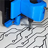
| Picture of the bench top plotter system plotting a circuit with graphite-loaded ink on paper. Other writing tools with different nanomaterials-based inks are placed at the bottom right part of the image. Copyright hold by the authors of the scientific article. (Image courtesy of the researchers)
|
|
“The technique is focused on increasing the impact of research groups that have expertise in creating solution-processable nanomaterials but lack the background or resources to print devices,” said Castellanos-Gomez. “With this simple route, these research groups can easily test their inks and prototype devices and sensors.”
|
|
Their method builds on recent advancements in solution-processable organic semiconductors, which have enabled the use of ink-printing lithographic techniques to create electronic devices more efficiently and cost-effectively. Various material families, such as nanotubes, nanowires, quantum dots, van der Waals materials, and hybrid perovskites, have been developed for compatibility with these techniques.
|
|
The researchers say that the technique is highly generalizable and that many other nanomaterial-based inks could be used. They demonstrated the potential of this technique by printing a variety of solution-processable nanomaterial inks, including van der Waals materials, quantum dots, hybrid organic-inorganic perovskites, and organic semiconductors. They illustrated the potential of this system with some applications like printing an invisible QR code using MoO3, a material that becomes opaque in UV light, or a photodetector on paper using a PEDOT organic semiconductor channel contacted by graphite electrodes.
|
|
While the technique works great on wettable substrates such as papers or textiles, more viscous inks and faster evaporation solvents are needed to print on plastics or glass. Nonetheless, the benchtop plotter used in the study cost less than 200 euros, a fraction of the cost of a traditional materials printer that can cost up to 60,000 euros.
|
|
“By using pens and a plotter, we have eliminated the need for expensive equipment and ink optimization, making printed electronics more accessible to researchers,” added Castellanos-Gomez. “We believe this technique has the potential to democratize printed electronics, enabling more widespread adoption and innovation in this exciting field.”
|
By
Michael
Berger
–
Michael is author of three books by the Royal Society of Chemistry:
Nano-Society: Pushing the Boundaries of Technology,
Nanotechnology: The Future is Tiny, and
Nanoengineering: The Skills and Tools Making Technology Invisible
Copyright ©
Nanowerk
|
|
|


