| Aug 10, 2022 |
|
(Nanowerk News) The ongoing fourth industrial revolution is data-driven and the optical interconnects are expected to feature higher bandwidth, smaller footprint, and lower power consumption to meet the dramatically growing demand for stronger data processing ability.
|
|
As a key element of the optical communication systems, a photodetector can convert the optical signal into the electrical signal and is expected to feature ultrahigh bandwidth.
|
|
Graphene/silicon hybrid photodetectors have attracted numerous attentions since its first demonstration due to its potential to realize bandwidth higher than 100 GHz. However, graphene’s atomic-thickness seriously limits its optical absorption thus causing low responsivity.
|
|
Plasmonic structures have been explored to enhance the responsivity, but the intrinsic metallic Ohmic absorption of the plasmonic mode limits its performance.
|
 |
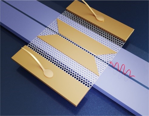
| The schematic of the double slot graphene photodetector. (Image courtesy of the researchers)
|
|
To address this issue, the authors of this article (Opto-Electronic Advances, “Graphene photodetector employing double slot structure with enhanced responsivity and large bandwidth”) propose a novel double slot structure for high-performance photodetection, taking advantages of both silicon photonics and plasmonics.
|
|
With the optimized structural parameters, the double slot structure significantly promotes graphene absorption while maintaining low metallic absorption. Based on the double slot structure, the demonstrated photodetector holds a high responsivity of 603.92 mA/W and a large bandwidth of 78 GHz.
|
|
The high-performance photodetector provides a competitive solution for the photodetector on silicon. Moreover, the double slot structure could be beneficial to a broader range of hybrid two-dimensional material/silicon devices to achieve stronger light-matter interaction with lower metallic absorption.
|


