| Feb 10, 2025 |
|
(Nanowerk News) Research teams from Southeast University, led by Professors Zhenhua Ni and Junpeng Lv, in collaboration with Professor Hongwei Liu from Nanjing Normal University and Professor Peng Zhou from Fudan University, have achieved a breakthrough in van der Waals light-emitting diodes (LEDs). Their innovative approach combines two-dimensional perovskite materials with low-temperature van der Waals transfer technology, resulting in a remarkable quantum efficiency of over 10% at room temperature.
|
|
Their findings are published in Science Advances (“Van der Waals integrated single-junction light-emitting diodes exceeding 10% quantum efficiency at room temperature”).
|
|
The development of optoelectronic integrated chips faces a critical challenge: the lack of high-performance on-chip light sources. Two-dimensional semiconductor materials have emerged as promising candidates for next-generation optoelectronic systems, offering superior properties and integration advantages. However, despite recent advances in two-dimensional semiconductor-based LED devices, their practical application in optoelectronic chips has been limited by low luminous efficiency at room temperature and under high injection conditions.
|
|
In this breakthrough study, the researchers leveraged two-dimensional semiconductor materials featuring multiple quantum wells, integrating them through low-temperature van der Waals transfer technology to create highly efficient on-chip LEDs. The team’s success stems from combining the advantages of two-dimensional perovskite multi-quantum well structure and its high fluorescence quantum yield with the low potential barrier height at the graphene/two-dimensional perovskite interface.
|
|
Through efficient carrier tunneling recombination, they achieved an external quantum efficiency exceeding 10% at room temperature—setting a new benchmark for van der Waals light-emitting diodes. This versatile approach can be adapted to other layered two-dimensional materials, paving the way for the development of large-area, high-efficiency, high-brightness integrated two-dimensional semiconductor light-emitting devices.
|
 |
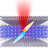
| Top: Schematics of the device fabrication process. Bottom left: Schematic cross-sectional illustration of the light emission process in the van der Waals LED device. Bottom right: Comparison of the EQE of our device to that of state-of-the-art vdWLEDs with various device structures at room temperature. Device structures of all kinds of vdWLEDs are schematically presented, including p-n junctions (PN), p-i-n junctions (PIN), transient LEDs (Transient), semiconductor-insulator-semiconductor (SIS), metal-insulator-semiconductor (MIS), and quantum wells (QW). (Image: Courtesy of the researchers)
|
|
The research represents a collaborative effort between multiple institutions, with Professors Zhenhua Ni and Junpeng Lv from Southeast University’s School of Electronic Science and Engineering and School of Physics, Professor Hongwei Liu from Nanjing Normal University’s School of Physics Science and Technology, and Professor Peng Zhou from Fudan University’s School of Microelectronics serving as co-corresponding authors. Zhenliang Hu, a postdoctoral fellow, and doctoral student Qiang Fu from Southeast University’s School of Physics are co-first authors.
|