| May 07, 2024 |
|
(Nanowerk News) In a new paper published in the journal Science Advances (“Unzipping hBN with ultrashort mid-infrared pulses”), researchers at Columbia Engineering used commercially available tabletop lasers to create tiny, atomically sharp nanostructures, or nanopatterns, in samples of a layered 2D material called hexagonal boron nitride (hBN).
|
|
While exploring potential applications of their nanopatterned structures with colleagues in the Physics Department, the team found that their laser-cut hBN samples could effectively create and capture quasiparticles called phonon-polaritons, which occur when atomic vibrations in a material combine with photons of light.
|
|
“Nanopatterning is a major component of material development,” explained engineering PhD student Cecilia Chen, who led the development of the technique. “If you want to turn a cool material with interesting properties into something that can perform specific functions, you need a way to modify and control it.”
|
|
The new nanopatterning technique, developed in the lab of Professor Alexander Gaeta, is a simple way to modify materials with light—and it doesn’t involve an expensive and resource-intensive clean room.
|
 |
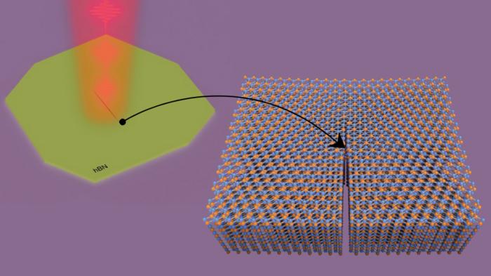
| The Gaeta Lab at Columbia Engineering “unzips” hexagonal boron nitride with a mid-infrared laser tuned to the material’s resonant frequency. The result is an atomically sharp line. (Image: The Gaeta Lab, Columbia Engineering)
|
A Nanoscale Paradox
|
|
Several well-established techniques exist to modify materials and create desired nanopatterns, but they tend to require extensive training and expensive overhead. Electron beam lithography machines, for example, must be housed in carefully controlled clean rooms, while existing laser options involve high heat and plasmas that can easily damage samples; the size of the laser itself also limits the size of the patterns that can be created.
|
|
The Gaeta lab’s technique takes advantage of what’s known in the optics and photonics community as “optical driving.” All materials vibrate at a particular resonance. Chen and her colleagues can enhance those vibrations by tuning their lasers to that frequency—corresponding to a wavelength of 7.3 micrometers, in the case of hBN—which they first demonstrated in research published last November in Nature Communications (“Phonon-enhanced nonlinearities in hexagonal boron nitride”).
|
|
In the newly published work, they pushed hBN to even more intense vibrations, but rather than damaging the underlying atomic structure, the lasers broke the crystal lattice cleanly apart. According to Chen, the effect was visible under the microscope and looked like unzipping a zipper.
|
|
The resulting lines across the sample were atomically sharp and much smaller – just a few nanometers – than the mid-infrared laser wavelengths used to create them.
|
|
“Usually, you need a shorter wavelength to make a smaller pattern,” said Chen. “Here, we can create very sharp nanostructures using very long wavelengths. It’s a paradoxical phenomenon.”
|
Small Structures, Big Physics
|
|
To explore what they could do with their nanopatterned samples, the engineering team teamed up with physicist Dmitri Basov’s lab, which specializes in creating and controlling nano-optical effects in different 2D materials – including creating phonon-polaritons in hBN. These vibrating quasiparticles can help scientists “see” beyond the diffraction limit of conventional microscopes and detect features in the material that give rise to quantum phenomena. They could also be a key component to miniaturizing optical devices, as electronics have become smaller over the years.
|
|
“Modern society is based on miniaturization, but it’s been much harder to shrink devices that rely on light than electrons,” explained physics PhD student and co-author Samuel Moore. “By harnessing strong hBN atomic vibrations, we can shrink infrared light wavelengths by orders of magnitude.”
|
|
Ultrasharp edges are needed to excite phonon-polaritons—normally, they are launched from the sides of flakes of hBN prepared via what’s known as the “Scotch tape” method, in which a bulk crystal is mechanically peeled into thinner layers using household tape. However, the team found that the laser-cut lines offer even more favorable conditions for creating the quasiparticles.
|
|
“It’s impressive how the laser-cut hBN regions launch phonon polaritons even more efficiently than the edge, suggesting an ultra-narrow unzipped hBN region that strongly interacts with infrared light,” said Moore.
|
|
As the new technique can create nanostructures anywhere on a sample, they also unzipped two lines in parallel. This creates a small cavity that can confine the phonon-polaritons in place, which enhances their nano-optical sensitivity. The team found that their unzipped cavities had comparable performance in capturing the quasiparticles to conventional cavities created in clean rooms.
|
|
“Our results suggest that our preliminary structures can compete with those created from more established methods,” noted Chen.
|
Escaping the Clean Room
|
|
The technique can create many customizable nanopatterns. Beyond two-line cavities, it can create any number of parallel lines. If such arrays can be produced on-demand with any desired spacings, it could greatly improve phonon-polaritons’ imaging ability and would be a huge achievement, said Moore.
|
|
A break can be extended as long as desired once started, and samples as thick as 80 nanometers and as thin as 24 nanometers have been unzipped – theoretically, the bound could be much lower. This gives researchers plenty of options to modify hBN and explore how its nanopatterning can influence its resulting properties, without having to gear up in a clean room bunny suit. “It really just depends on your ultimate goal,” said Chen.
|
|
That said, she still sees plenty of room to improve. Because hBN is a series of repeating hexagons, the technique only produces straight or angled lines meeting at either 60° or 120° at the moment, though Chen thinks combining them into triangles should be possible. Currently, the breaks can only occur in-plane as well; if they can determine how to target out-of-plane vibrations, they could potentially shave a bulk crystal down into different three-dimensional shapes. They are also limited by the power of their lasers, which they spent years carefully tuning to work stably at the desired wavelengths. While their mid-IR setup is well-suited to modifying hBN, different lasers would be needed to modify materials with different resonances.
|
|
Regardless, Chen is excited about the team’s concept and what it might be able to do in the future. As a member of the ultrafast-laser subgroup in the Gaeta Lab, Chen helped with their transition from creating and studying high-powered lasers to using those as tools to probe the optical properties of 2D materials.
|
|
That problem shared similarities to other problems Chen tackles in her time outside the lab as a boulderer, a form of rock climbing in which climbers scrabble up low, rugged rock faces without harness equipment to catch them if they fall.
|
|
“In bouldering, the potential climbing routes are called problems, and there’s no right answer to solving them,” she said. The best solutions cannot be brute forced, she continued: “You have to come up with a plan or you won’t be successful, whether figuring out how to exploit macroscopic features in a boulder or microscopic ones in a tiny crystal.”
|


