| Nov 23, 2023 |
|
(Nanowerk News) The University of Ottawa, together with national and international partners, has achieved a world first by manufacturing the first back-contact micrometric photovoltaic cells.
|
|
This innovative achievement is described in more detail in Cell Reports Physical Science (“3D interconnects for III-V semiconductor heterostructures for miniaturized power devices”).
|
Key Takeaways
|
|
World-first achievement in manufacturing back-contact micrometric photovoltaic cells, offering significant improvements over traditional solar technologies.
These cells feature reduced shadowing and potential for threefold lower energy production costs, contributing to advancements in electronic device miniaturization.
The innovation holds promise for diverse applications, including solar cells, space exploration batteries, and telecommunication device miniaturization, indicating a leap towards more efficient and powerful technology.
|
 |
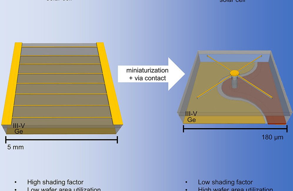
| Photo showing the difference between a standard solar cell and a miniaturized solar cell. (Image: University of Ottawa)
|
The Research
|
|
The cells, with a size twice the thickness of a strand of hair, have significant advantages over conventional solar technologies, reducing electrode-induced shadowing by 95% and potentially lowering energy production costs by up to three times.
|
|
The technological breakthrough—led by Mathieu de Lafontaine, a postdoctoral researcher at the University of Ottawa and a part-time physics professor; and Karin Hinzer, vice-dean, research, and University Research Chair in Photonic Devices for Energy at the Faculty of Engineering—paves the way for a new era of miniaturization in the field of electronic devices.
|
|
The micrometric photovoltaic cell manufacturing process involved a partnership between the University of Ottawa, the Université de Sherbrooke in Quebec and the Laboratoire des Technologies de la Microélectronique in Grenoble, France.
|
|
“These micrometric photovoltaic cells have remarkable characteristics, including an extremely small size and significantly reduced shadowing. Those properties lend themselves to various applications, from densification of electronic devices to areas such as solar cells, lightweight nuclear batteries for space exploration and miniaturization of devices for telecommunications and the internet of things,” Hinzer says.
|
A breakthrough with huge potential
|
|
“This technological breakthrough promises significant benefits for society. Less expensive, more powerful solar cells will help accelerate the energy shift. Lightweight nuclear batteries will facilitate space exploration, and miniaturization of devices will contribute to the growth of the internet of things and lead to more powerful computers and smartphones,” de Lafontaine says.
|
|
“The development of these first back-contact micrometric photovoltaic cells is a crucial step in the miniaturization of electronic devices,” he adds.
|
|
“Semiconductors are vital in the shift to a carbon-neutral economy. This project is one of many research initiatives that we’re undertaking at the Faculty of Engineering to achieve our societal goals,” says Hinzer. Semiconductors are included in three of the five research areas at the Faculty of Engineering, namely, information technologies, photonics and emerging materials, and two of the four strategic areas of research at the University of Ottawa, namely, creating a sustainable environment and shaping the digital world.
|
|
This international partnership between Canada and France illustrates the importance of innovation and research in micromanufacturing, leading the way to a future in which technology will become more powerful and accessible than ever. It also marks an historic step in the evolution of the global scientific and technology scene.
|


