| Dec 04, 2023 |
|
(Nanowerk News) The properties that make materials like semiconductors so sought after result from the way their atoms are connected, and insight into these atomic configurations can help scientists design new materials or use existing materials in new, unforeseen ways.
|
|
Rice University materials scientist Yimo Han and collaborators mapped out the structural features of a 2D ferroelectric material made of tin and selenium atoms, showing how domains ⎯ areas of the material in which molecules are identically oriented ⎯ impact the behavior of the material.
|
 |
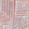
| Rice researchers used four-dimensional scanning transmission electron microscopy to analyze the structure of the material (first panel from left); their analysis yielded a ferroelastic strain map of a flake of the material (second and third panels). Insets on the third panel represent polarization directions in different stripe domains. (Image: Han lab/Rice University)
|
|
“Ferroelectric materials are widely used in applications such as memories and sensors, and they will likely be increasingly useful for building next-generation nanoelectronics and in-memory computing,” said Chuqiao Shi, a Rice graduate student in the Han lab and lead author on a study published in Nature Communications (“Domain-dependent strain and stacking in two-dimensional van der Waals ferroelectrics”). “That’s because 2D ferroelectric materials have remarkable properties and are characterized by their atomic thinness and enhanced integration capabilities.”
|
|
In ferroelectric materials, molecules are polarized, and they also segregate and align based on polarization. Moreover, 2D ferroelectrics change shape in response to electrical stimuli ⎯ a phenomenon known as flexoelectricity. In the tin-selenium crystal that is the focus of this research, molecules self-organize into patches or domains, and the flexoelectric effect causes these to move, giving rise to structural shifts in the material that impact its properties and behavior.
|
|
“It’s really important that we understand the intricate relationship between atomic structure and electric polarization, which is a critical feature in ferroelectric materials,” said Han, an assistant professor of materials science and nanoengineering. “This domain-dependent structure can be very useful for engineers to figure out how to best use the material and rely on its properties to design applications.”
|
|
Unlike conventional ferroelectrics in which atoms are bound by a rigid lattice, in the tin-selenite crystal studied by Han and Shi, the forces that bind the atoms together are weaker, giving the atomic lattice a more supple and pliant quality.
|
|
“The material belongs to a special class of 2D materials known as van der Waals ferroelectrics, whose properties could serve to design next-generation, ultra-thin data storage devices and sensors,” Shi said. “Van der Waals forces are weaker than chemical bonds ⎯ they’re the same kind of forces that allow geckos to defy gravity and climb walls.
|
|
“The soft in-plane lattices of this 2D material coupled with relatively weaker interlayer van der Waals forces give rise to a unique structural landscape. These distinctive structural features generate effects exclusive to 2D ferroelectrics that are absent in their bulk counterparts.”
|
|
The greater degree of flexibility or freedom of the atomic lattice in 2D van der Waals ferroelectrics makes it more difficult to map out the relationship between polarization and material structure.
|
|
“In our study, we developed a new technique that allows us to look at both in-plane strain and out-of-plane stacking order simultaneously, which is something conventional investigations of this material were unable to do previously,” Han said. “Our findings are set to revolutionize domain engineering in 2D van der Waals ferroelectrics and position them as fundamental building blocks in the development of advanced devices for the future,” Han said.
|


