| Mar 23, 2022 |
|
(Nanowerk News) Metallic materials used in engineering must be strong and ductile – capable of carrying high mechanical loads while able to withstand deformation without breaking. Whether a material is weak or strong, ductile or brittle, however, is not determined simply by the crystal grains that make up the material, but rather by what happens in the space between them known as the grain boundary.
|
|
Despite decades of investigation, atomic-level deformation processes at the grain boundary remain elusive, along with the secret to making new and better materials.
|
|
Using advanced microscopy coupled with novel computer simulations that track atomic movement, researchers at the Georgia Institute of Technology conducted real-time atomic-level observations of grain boundary deformation in poly-grained metallic materials called polycrystalline materials. The team observed previously unrecognized processes that affect material properties, such as atoms that hop from one plane to another across a grain boundary.
|
 |
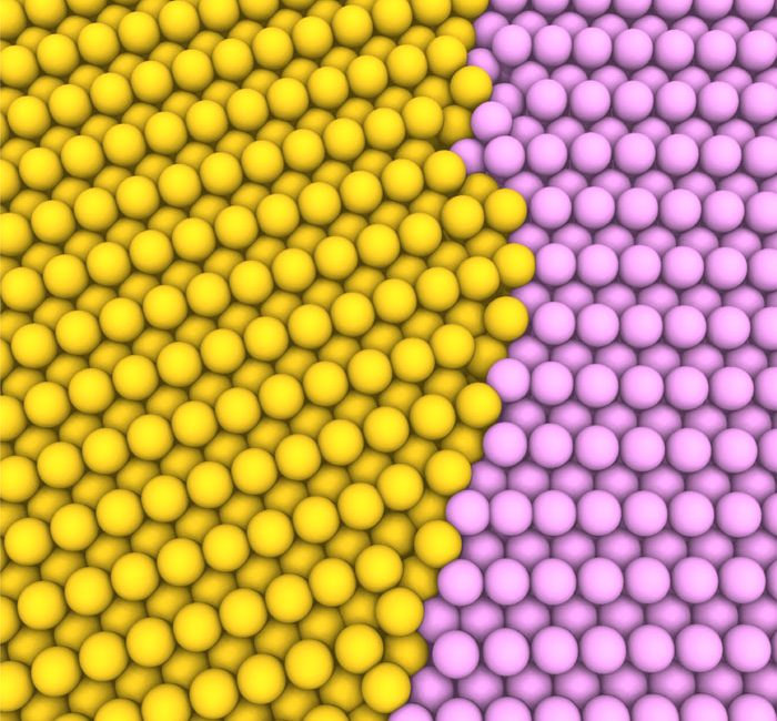
| Electron microscopy reveals how the sliding deformation of grain boundaries is accomplished atom by atom in a poly-grained metal of platinum. The graphic shows the atomic structure of a grain boundary between two abutting grains where platinum atoms are colored in yellow and pink, respectively. (Image: Georgia Tech)
|
|
Their work, published in Science (“Tracking the sliding of grain boundaries at the atomic scale”), pushes the limits of atomic-level probing, and enables a deeper understanding of how polycrystalline materials deform. Their work opens new avenues for the smarter design of new materials for extreme engineering applications.
|
|
“It is amazing to observe the step-by-step movements of atoms, and then use this information to decipher the dynamic sliding process of a grain boundary with complex structure,” said Ting Zhu, professor in the George W. Woodruff School of Mechanical Engineering and one of the lead authors on the study, which included collaborators from Beijing University of Technology.
|
|
To develop new and better polycrystalline materials, it is critical to understand how they deform at an atomic level. The team sought to achieve real-time observation of grain boundary sliding, a well-known mode of deformation which plays an important role in governing the strength and ductility of polycrystalline materials. They chose to work with platinum because its crystal structure is the same as other widely used polycrystalline materials like steel, copper, and aluminum. Using platinum, their results and insights would be generally applicable to a wide range of materials.
|
A Combination of Novel Methods
|
|
Several key innovations were required to carry out the experiment. The team used a transmission electron microscope (TEM) to capture highly magnified images of atoms at grain boundaries. The TEM sends an electron beam through a film-like platinum specimen, processed by the team to be thin enough for electron transmission. They also developed a small, millimeter-sized testing device that applies mechanical force to a specimen and is affixed to the microscope. The TEM and device work in tandem to create atomic-level images of grain boundaries during deformation.
|
|
To observe the atomic-scale grain boundary sliding more clearly than through viewing the TEM images alone, the researchers developed an automated atom tracking method. This method automatically labels each atom in every TEM image and then correlates them between images, enabling the tracking of all atoms and their movement during grain boundary sliding.
|
|
Finally, the team conducted computer simulations of grain boundary sliding using atomic structures extracted from the TEM images. The simulated sliding helped the team analyze and interpret events that happened at the atomic scale. By combining those methods, they were able to visualize how individual atoms move at a deforming grain boundary in real time.
|
Results
|
|
While it was known that grain boundaries slide during deformation of polycrystalline materials, real-time imaging and analysis by Zhu and his team revealed a rich variety of atomic processes, some of them previously unknown.
|
|
They noticed that, during deformation, two neighboring grains slid against each other and caused atoms from one side of the grain boundary plane to transfer to the other. This process, known as atomic plane transfer, was previously unrecognized. They also observed that local atomic processes can effectively accommodate transferred atoms by adjusting grain boundary structures, which can be beneficial for achieving higher ductility.
|
|
Image analysis and computer simulations showed that mechanical loads were high during the atomic processes, and that this facilitated the transfer of atoms and atomic planes. Their findings suggest that engineering the grain boundaries of fine-grained polycrystals is an important strategy for making materials stronger and more ductile. |
Looking Ahead
|
|
Zhu and his team’s demonstrated ability to observe, track, and understand atomic-scale grain boundary deformation opens more research opportunities to further investigate interfaces and failure mechanisms in polycrystalline materials. Greater understanding of atomic-level deformation can inform how materials are evolved during grain boundary engineering, a necessity for creating exceptional strength and ductility combinations.
|
|
“We are now extending our approach to visualize atomic-scale deformation at higher temperatures and deformation rates, in pursuit of better materials for extreme applications,” said Xiaodong Han, another lead author of the paper and a professor at the Beijing University of Technology.
|
|
Zhu believes that the data-rich results from their real-time atomic-level observations and imaging could be integrated with machine learning for deeper investigation of material deformations, and this could accelerate the discovery and development of materials faster than previously thought possible.
|
|
“Our work shows the importance of using very high-resolution microscopy to understand atomic-level material behavior. This advancement will enable researchers to tailor materials for optimal properties using atomic design,” said Zhu.
|


