| Apr 27, 2020 |
|
(Nanowerk News) The duration of their snapshot relates to one second as one second relates to the age of the universe: In a joint collaboration with Australian Scientist Tim Davis and the Group around Harald Gieen (University of Stuttgart), Physicists from CENIDE have developed ultrafast vector microscopy as a way of determining electric fields on surfaces with high temporal and spatial resolution. The new method was used to measure the dynamics of optical skyrmions in the time domain for the first time.
|
|
The renowned journal Science publishes this breakthrough in nanooptics (“Ultrafast vector imaging of plasmonic skyrmion dynamics with deep subwavelength resolution”).
|
 |
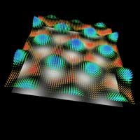
| Visualization of optical skyrmions at a point in time when their electric fields in the center point out of the surface. The distance between adjacent skyrmions is the plasmon wavelength of 780 nanometers. (Image: Tim Davis)
|
|
Nanooptics is all about interactions between light and matter. Researchers engaged in this field use spectroscopic and microscopic methods to observe and influence the properties and states of tiny structures and even individual molecules. Like with optical computers, which are still in their infancy: their structures can be far smaller than the wavelength of light, and they require tricks such as nano-antennas to couple light into nanostructures effectively. However, it is quite challenging to analyze the electric fields around such structures in space and time.
|
|
A team of physicists led by Professor Frank-J. Meyer zu Heringdorf (UDE), the Australian nanooptics expert Dr. Timothy J. Davis, and Professor Harald Gieen (University of Stuttgart) have now realized a pioneering achievement: With their vector microscopy, based on time-resolved 2-photon photoemission microscopy, they have been able to analyze the electrical fields on a metal surface with pinpoint accuracy and temporal precision down to 10 nanometers of local resolution and in a range of sub-femtoseconds.
|
Ultra-short laser pulses combined with vector analysis
|
|
For this purpose, they used gold microcrystallites with a specifically nanostructured surface. They then used an ultrashort laser pulse to generate a surface plasmon polariton, which is an electron wave that propagates on the surface. A few femtoseconds after excitation, a second pulse was used to probe the electric field of the wave. Yet the probe pulse can only analyze the component that is equally polarized, i.e., where the electric field of the probe pulse and that of the plasmon on the surface point in the same direction.
|
|
The scientists reconstructed the field vectors by determining two field components perpendicular to each other in two single experiments with different probing polarizations. The third component of the field was subsequently calculated using Maxwell’s equations. “This is a real breakthrough, says Meyer zu Heringdorf, who is also a member of UDE’s Collaborative Research Centre, “Non-equilibrium dynamics of condensed matter in the time domain.” “This means that every point of an electric field on a surface can be observed at any time even in the tiniest structures.”
|
Oscillating skyrmions observed
|
|
Due to their promising properties in magnetic systems, researchers are currently investigating whether the magnetic properties of skyrmions can also be transferred to optics. The physicists have therefore demonstrated the value of their newly developed method by investigating the sub-femtosecond dynamics of optical skyrmions for the first time.
|
|
To this end, the team created plasmons on the gold surface whose electric fields formed optical skyrmions (see image). They then systematically increased the time interval between pump and probe laser pulses by about 100 attoseconds. The sequence of the reconstructed vector images results in a movie of how the field in the optical skyrmion is oscillating up and down.
|
|
Since the method is generally applicable to electric fields on surfaces, vector microscopy can be used to study field distributions in optical nanostructures with a precision that would have been unthinkable just a few years ago.
|


